Packaging structure of luminous semiconductor chip and packaging method thereof

A light-emitting semiconductor and packaging structure technology, which is applied in the field of lighting, can solve the problems of reducing luminous efficiency, limiting the scope of use, and difficulty in the amount of glue, and achieves the effects of improving the heat dissipation environment, popularizing and using a wide range of applications

Inactive Publication Date: 2011-02-16
敬俊
View PDF9 Cites 6 Cited by
  • Summary
  • Abstract
  • Description
  • Claims
  • Application Information

AI Technical Summary

Problems solved by technology

But there are still some deficiencies: 1. After the glue is sealed, the light-emitting semiconductor chip can only dissipate heat from the bottom, and a large-volume radiator needs to be used to ensure its normal working temperature, while a large-volume radiator made of metal requires High manufacturing cost, and due to the large volume of the radiator, the installation of its finished product is limited by physical conditions, which limits its scope of use
2. The fluorescent powder is directly coated on the surface of the chip. Due to the existence of light scattering, the light extraction efficiency is low
3. After the phosphor coating is potted with epoxy resin, its heat dissipation performance is poor. It is exposed to ultraviolet radiation for a long time, and it is prone to temperature quenching and aging, which reduces the luminous efficiency.
At the same time, due to the mismatch between the refractive index of the phosphor powder and the epoxy resin, the refraction effect of the phosphor powder on light is reduced
4. During the operation of sealing glue (epoxy resin), it is difficult to control the amount of glue. For example, there are strict requirements on the height of the glue and the position of glue dispensing, otherwise the light effect will be affected; in addition, the epoxy resin will be damaged during use. Thickening, resulting in phosphor precipitation, resulting in the problem of chromatic aberration
5. The heat dissipation and heat resistance of epoxy resin are poor. Often before the life of the semiconductor core itself is reached, the epoxy resin will change color and affect the light output effect.

Method used


Image

  • Packaging structure of luminous semiconductor chip and packaging method thereof
  • Packaging structure of luminous semiconductor chip and packaging method thereof
  • Packaging structure of luminous semiconductor chip and packaging method thereof

Examples


Embodiment 1

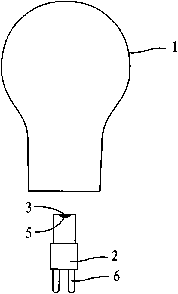
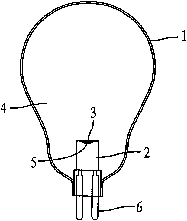
[0026] Such as Figures 1 to 6 As shown, the packaging structure of the light-emitting semiconductor chip according to the present invention includes a light-emitting semiconductor chip 3 and a lampshade 1. The light-emitting semiconductor chip 3 is fixed on the light-emitting semiconductor chip bracket 2, and the light-emitting semiconductor chip bracket 2 and The light-emitting semiconductor chip bracket 2 is electrically connected to the power supply according to the connection mode of the existing LED lamps, such as two pins 6 protruding from its lower part are electrically connected to the power supply; the lower end of the lampshade 1 is open, and it passes through the opening. It is fixedly connected with the light-emitting semiconductor chip bracket 2 to form a closed cavity 4, so that the light-emitting semiconductor chip 3 is located in the closed cavity 4, isolated from the outside world and oxygen, not easy to be oxidized, and can also prevent moisture. The light-e...

Embodiment 2

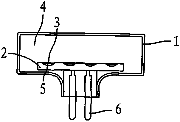
[0040] Such as Figure 7 As shown, the packaging structure of the light-emitting semiconductor chip according to the present invention includes a light-emitting semiconductor chip 3 and a lampshade 1. The light-emitting semiconductor chip 3 is fixed on the light-emitting semiconductor chip bracket 2; Composed with the transparent cover 9, the lower part of the lamp cup 8 is fixedly connected with the light-emitting semiconductor chip bracket, the upper end of the lamp cup is open, and it is fixedly connected with the transparent cover 9 through the opening to form a closed cavity 4, and the light-emitting semiconductor chip 3 is located in the cavity 4. The light-emitting semiconductor chip 3 is isolated from the outside world and oxygen, not easy to be oxidized, and also moisture-proof. The surface of the light-emitting semiconductor chip bracket 2 can be flat, inwardly recessed arc-shaped or irregular, and the light-emitting semiconductor chips 3 are evenly distributed on th...


PUM


Abstract

The invention discloses a packaging structure of a luminous semiconductor chip and a packaging method thereof. The packaging structure of the luminous semiconductor chip comprises the luminous semiconductor chip and a lampshade, wherein the luminous semiconductor chip is fixed on the bracket of the luminous semiconductor chip; the lampshade and the bracket of the luminous semiconductor chip are fixedly connected and form a sealed cavity; and the luminous semiconductor chip is positioned in the cavity. The lampshade and the bracket of the luminous semiconductor chip of the invention form the sealed cavity to isolate the luminous semiconductor chip from outside and oxygen, so that the luminous semiconductor chip has less possibility of being affected with damp and oxidized, and the packaging structure can be in nude packing without encapsulation by epoxy resin, thus the luminous semiconductor chip can radiate the heat from each direction so as to greatly improve the heat dissipation environment of the luminous semiconductor chip, and the luminous semiconductor chip has normal working temperature without a radiator. Thus, the packaging structure has low manufacture cost, is favourable for popularizing and using products, has simple packaging technology and is favourable for the mass production of the product.

Description

technical field [0001] The invention relates to the technical field of lighting, in particular to a packaging structure and packaging method of a light-emitting semiconductor chip for lighting. Background technique [0002] When the light-emitting semiconductor chip (LED) is exposed to emit light, it is easily oxidized and its service life is affected. In order to protect the light-emitting semiconductor chip, it is necessary to package the light-emitting semiconductor chip during the production process, and require the light-emitting semiconductor chip to be able to transmit light after packaging. Obviously, the packaging effect of the light-emitting semiconductor chip directly affects the service life of the LED lamp and the light output effect. . [0003] At present, a common packaging method of light-emitting semiconductor chips is as follows: placing the light-emitting semiconductor chip on a support, then dot-coating phosphor on the surface of the light-emitting semic...

Claims


Application Information

Patent Timeline
Patent Type & Authority Applications(China)
IPC IPC(8): F21S2/00F21V23/00H01L33/48F21V9/10F21V3/04F21V7/00F21V29/00H01L33/64F21V19/00F21V3/02F21Y101/02F21V9/40F21V29/503
Inventor 敬俊林娇燕
Owner 敬俊
Why Eureka
Try Eureka