Preparation method of OLED panel polycrystalline silicon
A production method and technology of polysilicon, applied in semiconductor/solid-state device manufacturing, electrical components, circuits, etc., can solve problems such as deterioration of TFT characteristics
- Summary
- Abstract
- Description
- Claims
- Application Information
AI Technical Summary
Problems solved by technology
Method used
Image

Examples
Embodiment Construction
[0041] The present invention will be further described below in conjunction with the accompanying drawings and specific embodiments.
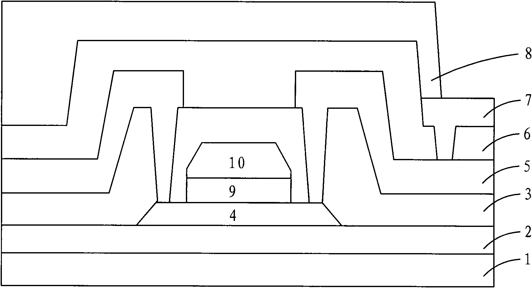
[0042] To make complete as figure 1 The AMOLED structure shown requires the following steps in sequence:
[0043] (1) After the glass substrate 1 is cleaned, a silicon oxide (SiOx) buffer layer 2 is deposited thereon by plasma enhanced chemical vapor deposition (PECVD).
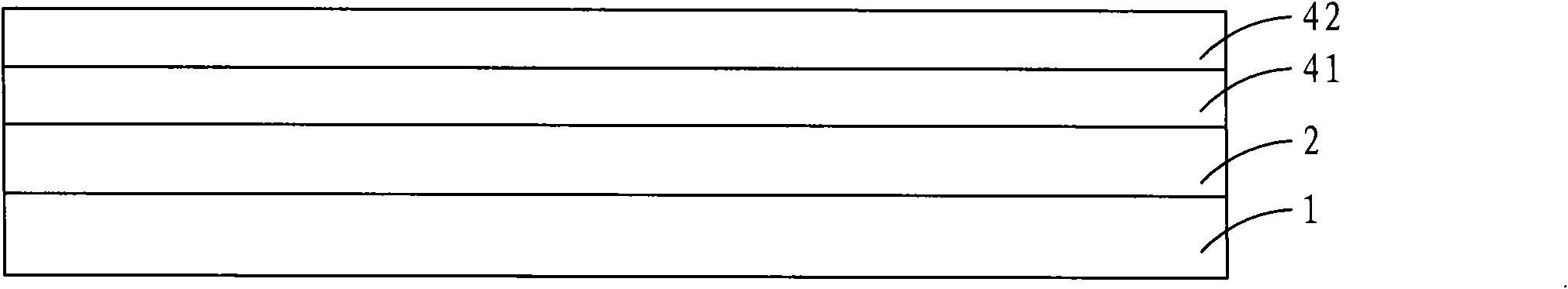
[0044] (2) Deposit 500 angstroms of amorphous silicon on the glass substrate 1 by low-pressure chemical vapor deposition (LPCVD) to form an amorphous silicon layer 41; the thickness of the amorphous silicon can be adjusted as required.
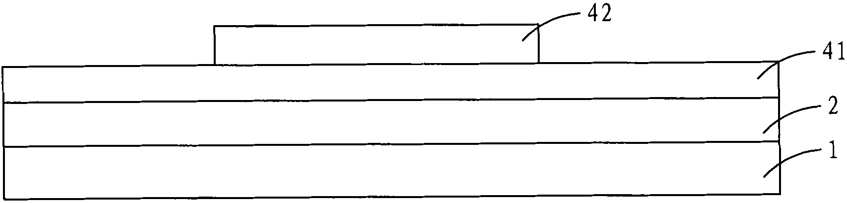
[0045] (3) Clean the glass substrate before photolithography, and evenly coat the photoresist layer 42 on the amorphous silicon layer 41. The thickness of the photoresist is 1.2 microns, forming such as figure 2 For the structure shown, the thickness of the photoresist can be adjusted as needed.
[0046] (4) photoresist is exposed and deve...
PUM
 Abstract
Description
Claims
Application Information
 - R&D
- Intellectual Property
- Life Sciences
- Materials
- Tech Scout
- Unparalleled Data Quality
- Higher Quality Content
- 60% Fewer Hallucinations
Browse by: Latest US Patents, China's latest patents, Technical Efficacy Thesaurus, Application Domain, Technology Topic, Popular Technical Reports.
© 2025 PatSnap. All rights reserved.Legal|Privacy policy|Modern Slavery Act Transparency Statement|Sitemap|About US| Contact US: help@patsnap.com