Method for improving conductivity of indium-doped zinc oxide transparent conductive film
A transparent conductive film, conductive performance technology, applied to the conductive layer on the insulating carrier, ion implantation plating, coating, etc., can solve the problem of low resistivity
- Summary
- Abstract
- Description
- Claims
- Application Information
AI Technical Summary
Problems solved by technology
Method used
Image
Examples
Embodiment 1
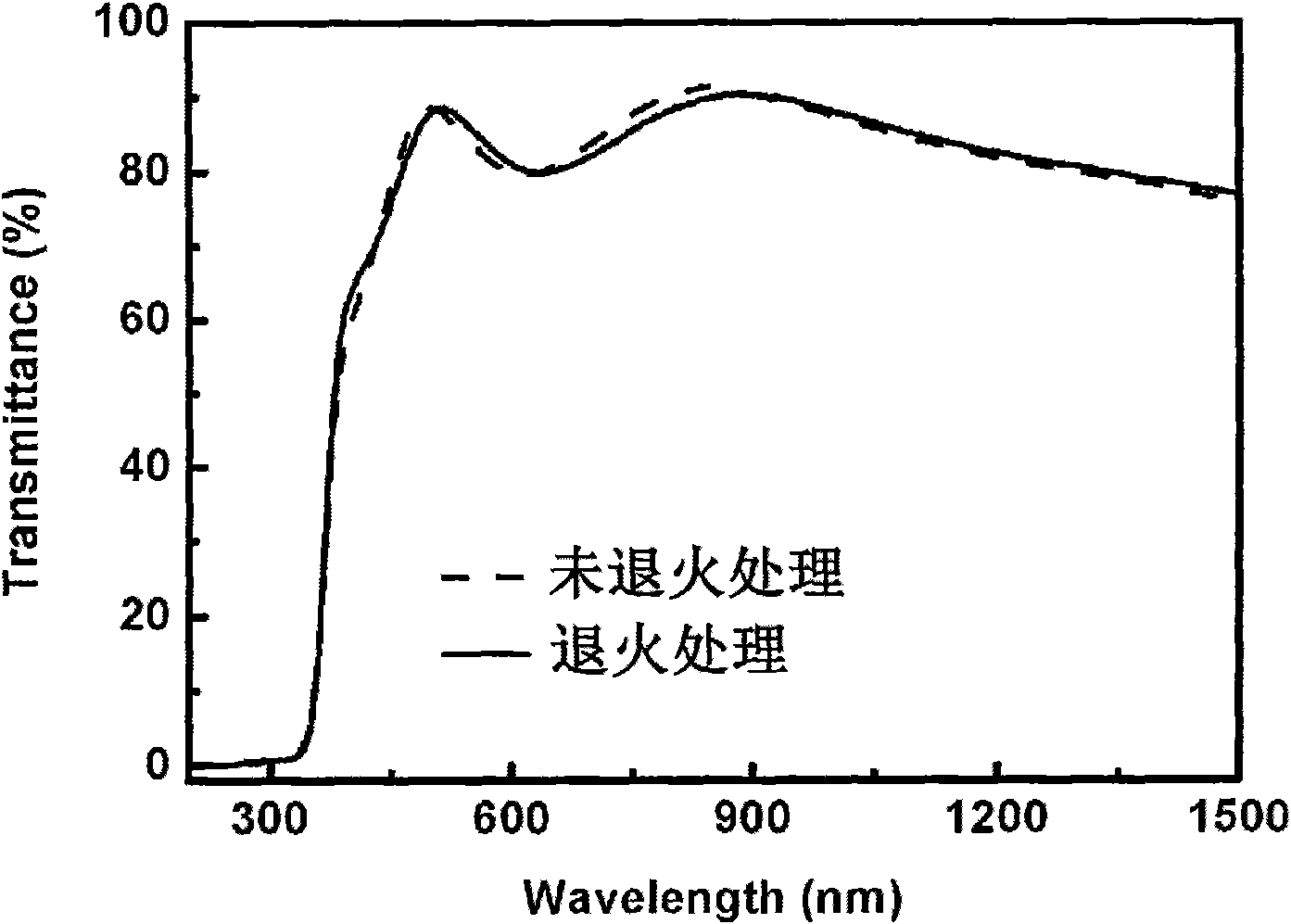
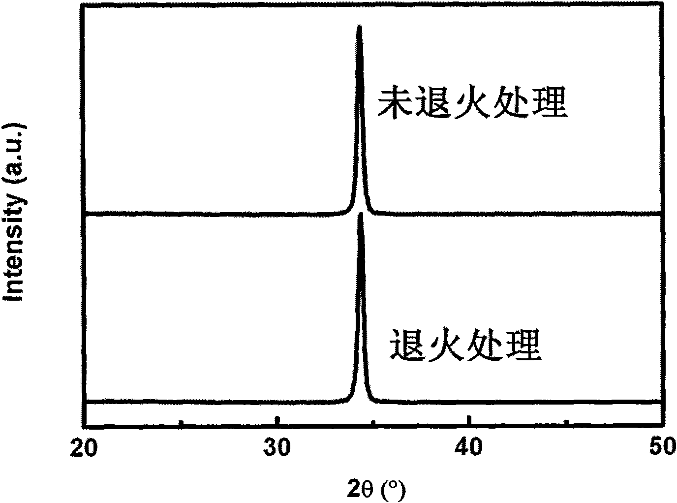
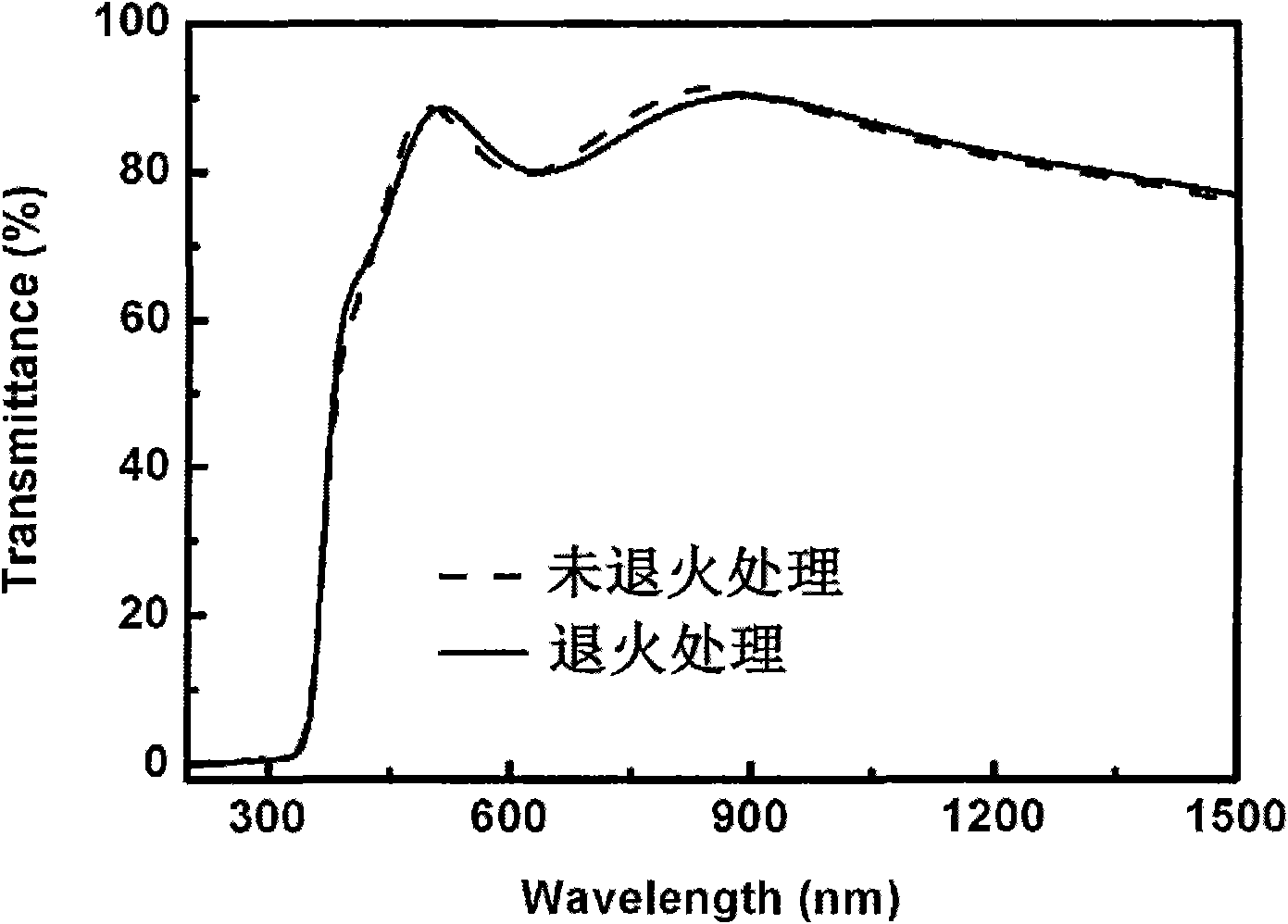
[0008] First, a zinc oxide ceramic target with a purity of 99.9% and an indium metal target are used to co-sputter and deposit an IZO transparent conductive film with a thickness of about 200nm by magnetron sputtering. is 0.5Pa, the background vacuum is 2×10 -4 Pa, the substrate temperature is 400°C, the RF sputtering power of ZnO target and Indium target is 10W / cm respectively 2 and 2W / cm 2 , the bias voltage is -100V, and the sample rotation speed is 6 rpm. Tests show that the atomic ratio of indium atoms to the sum of indium atoms and zinc atoms in the IZO transparent conductive film [In / (In+Zn)]≈3.5%, the indium content is very low, and its crystal structure is along the (002) orientation Hexagonal wurtzite phase structure, resistivity 1.3×10 -3 Ωcm, the carrier concentration is 1.1×10 21 / cm 3 , with a mobility of 4.53cm 2 V -1 S -1 , the transmittance is ~ 85% (400 ~ 1500nm).
[0009] Then put the prepared IZO transparent conductive film into the annealing furna...
PUM
| Property | Measurement | Unit |
|---|---|---|
| thickness | aaaaa | aaaaa |
| carrier concentration | aaaaa | aaaaa |
Abstract
Description
Claims
Application Information


