Nitrided barrier layers for solar cells

A solar cell and dielectric layer technology, applied in the field of solar cells, can solve problems such as damage to thinner wafers

Inactive Publication Date: 2011-03-30
APPLIED MATERIALS INC
View PDF1 Cites 15 Cited by
  • Summary
  • Abstract
  • Description
  • Claims
  • Application Information

AI Technical Summary

Problems solved by technology

This is adequate for thicker wafers (>200 microns thick), but causes unacceptable damage to thinner wafers

Method used


Image

  • Nitrided barrier layers for solar cells
  • Nitrided barrier layers for solar cells
  • Nitrided barrier layers for solar cells

Examples


Embodiment Construction

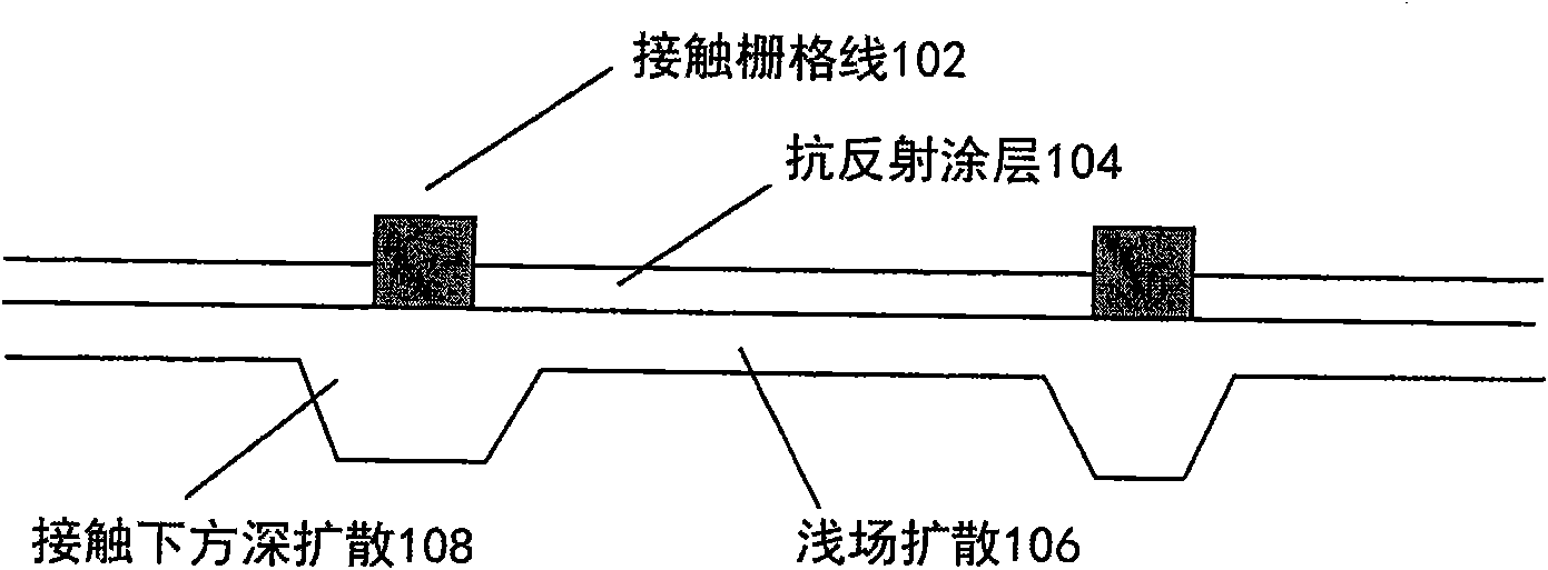
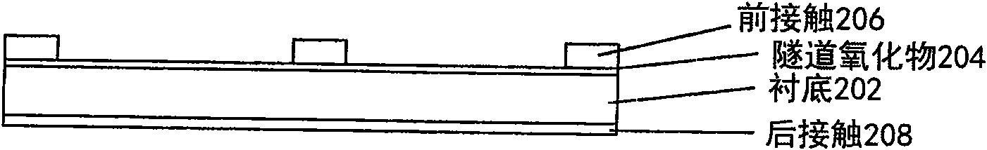
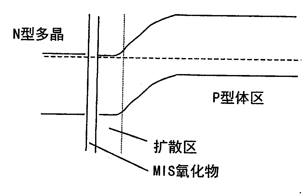
[0028] The present invention will now be described in detail with reference to the accompanying drawings, which are provided as illustrative examples to enable those skilled in the art to practice the invention. Obviously, the following figures and examples are not intended to limit the scope of the invention to a single embodiment, and that other embodiments are possible by interchange of some or all of the described or shown elements. Furthermore, when some elements of the present invention can be partially or fully implemented using known components, only those parts of such known components necessary for an understanding of the present invention will be described, and detailed descriptions of other parts of such known components will be omitted. described so as not to obscure the invention. In this specification, an embodiment showing a single component should not be considered limiting; rather, the invention is intended to encompass other embodiments comprising a pluralit...


PUM


Abstract

The present invention relates to polysilicon emitter solar cells, and more particularly to polysilicon emitter solar cells with hyperabrupt junctions, and methods for making such solar cells. According to one aspect, a polysilicon emitter solar cell according to the invention includes a nitrided tunnel insulator. The nitridation prevents boron diffusion, enabling a hyperabrupt junction for a p-poly on n-Si device. According to another aspect, a nitrided oxide (DPN) is used in a tunnel oxide layer of a MIS solar cell structure. The DPN layer minimizes plasma damage, resulting in improved interface properties. An overlying polysilicon emitter can then provide a low sheet resistance emitter without heavy doping effects in the substrate, excess recombination, or absorption, and is a significant improvement over a conventional diffused emitter or TCO. According to another aspect, the invention includes a method for making a solar cell structure that is functionally equivalent to a selective emitter, but without the requirement for multiple diffusions, long diffusions, aligned lithography, or fine contact holes.

Description

[0001] Cross References to Related Applications [0002] This application claims priority from US Provisional Application 61 / 043,664 and US Provisional Application 61 / 043,675, the entire contents of which applications are incorporated herein by reference. technical field [0003] The present invention relates to solar cells, and more particularly to solar cells having nitride junctions. Background technique [0004] Many types of solar cells have structures that have better junction and contact properties that can be improved due to the materials used and / or their fabrication processes. [0005] For example, polysilicon emitter solar cells have been available since the early 80's. It typically consists of polysilicon deposited on a thin tunnel dielectric such as silicon dioxide. The dielectric is supposed to perform two functions. First, it aims to passivate the interface between the polysilicon and the substrate. Second, it is designed to block diffusion to form hyperab...

Claims


Application Information

Patent Timeline
Patent Type & Authority Applications(China)
IPC IPC(8): H01L31/042
CPCH01L31/062Y02E10/547H01L31/1804Y02P70/50
Inventor 皮特·G·博登
Owner APPLIED MATERIALS INC
Why Eureka
Try Eureka