Semiconductor wafer grinding force on-line measurement device and force-controlling grinding method

A measuring device and grinding force technology, applied in the direction of grinding machine parts, grinding/polishing equipment, workpiece feed movement control, etc., to achieve the effect of high rigidity, less links, and small hysteresis

Active Publication Date: 2011-04-13
宁波知行半导体有限公司
View PDF4 Cites 38 Cited by
  • Summary
  • Abstract
  • Description
  • Claims
  • Application Information

AI Technical Summary

Problems solved by technology

[0006] The invention aims at the contradiction between processing efficiency and surface quality in the ultra-precision grinding process of semiconductor wafers and the problem of how to obtain high-precision wafer surfaces, combining the structural characteristics of the developed wafer grinder and the interaction between the grinding wheel and the wafer in the grinding process According to the distribution of force, a piezoelectric grinding force online measuring device is proposed to monitor the three-way grinding force dynamically in real time, and the wafer grinding method and implementation device are used to control the feed speed and feed rate through the feedback of the measured value. For efficient grinding and constant force grinding of semiconductor wafers

Method used


Image

  • Semiconductor wafer grinding force on-line measurement device and force-controlling grinding method
  • Semiconductor wafer grinding force on-line measurement device and force-controlling grinding method
  • Semiconductor wafer grinding force on-line measurement device and force-controlling grinding method

Examples


example

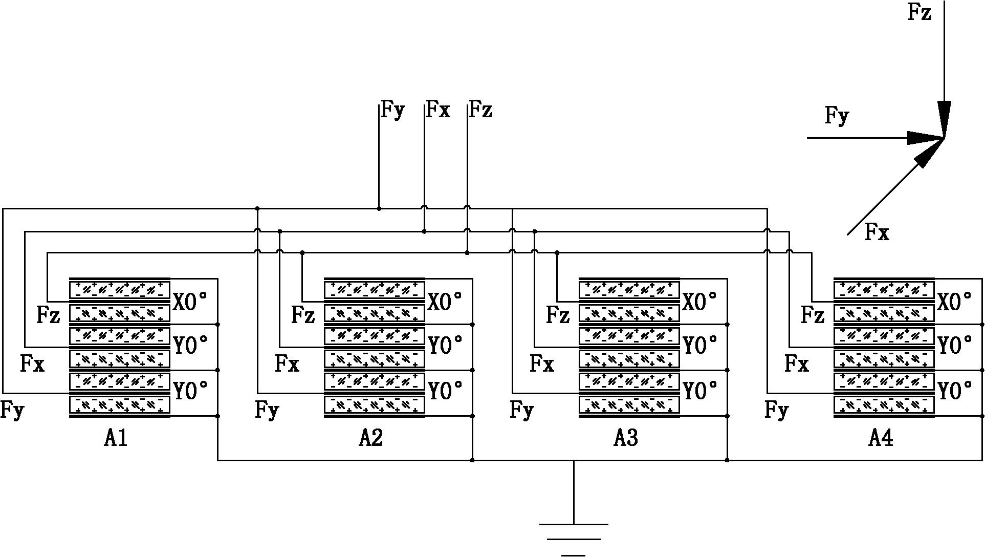
[0029] Example: The laboratory room temperature is 26°C, the sensitivities of the charge amplifier YE5850B are SX=7.93pc / kgf, SY=7.85pc / kgf, SZ=3.53pc / kgf respectively. It can be concluded from Table 1 that when Fz is loaded, the non-linear error is less than 0.2%, the repeatability error is less than 0.5%, and the cross-directional interference is less than 2%. The test results show that all the indicators have reached the standards stipulated by the International Production Engineering Research Association - Cutting Science and Technology Committee.

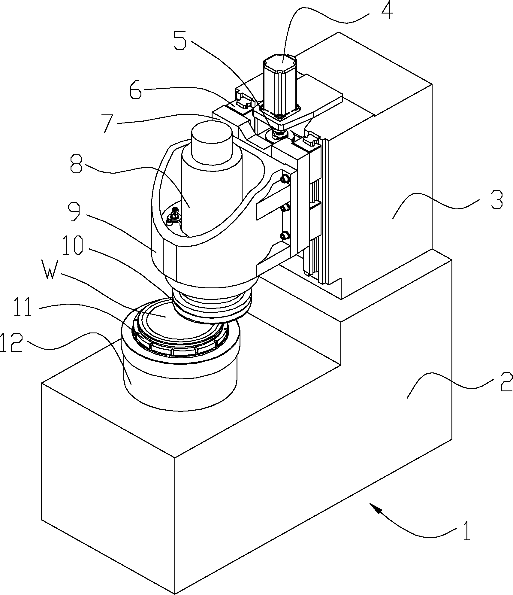
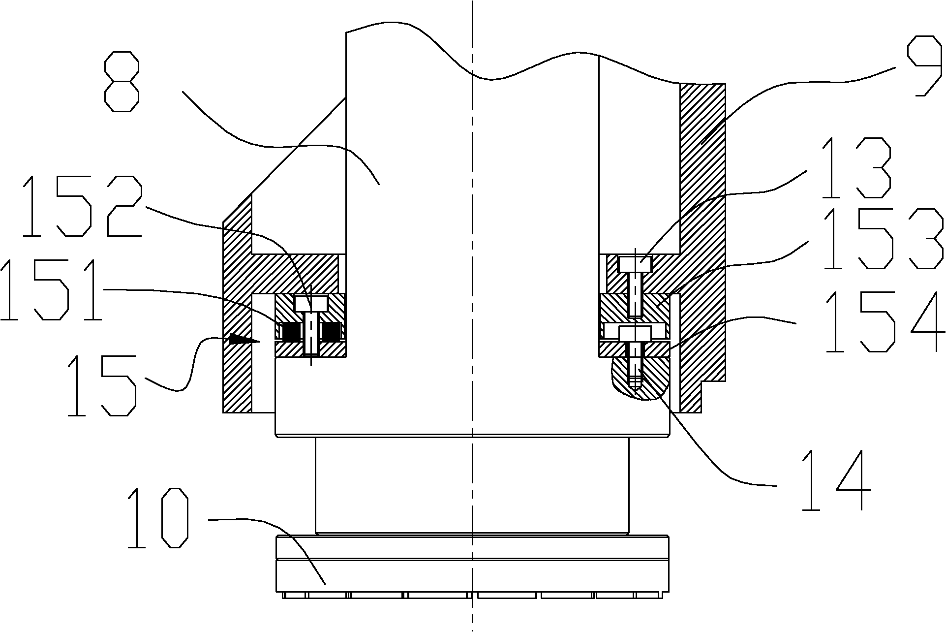
[0030] like Figure 4 As shown, when grinding a semiconductor wafer W, the grinding force is transmitted to the main shaft 8 through the grinding wheel 10, and then transmitted to the grinding force detection device 15 through the flange of the main shaft 8, and the corresponding radial force Fr and tangential force Ft are output respectively. and the charge signal of the axial force Fz are modulated and amplified by the data ...


PUM


Abstract

The invention belongs to the ultraprecision machining field of the hard and brittle semiconductor crystalline materials and relates to a grinding force on-line measurement device used in the grinding process of the semiconductor wafer and a force-controlling grinding method. The invention discloses a semiconductor wafer grinding force on-line measurement device which is used as the feedback element of a grinding force adaptive control system. The grinding force measurement device adopts the piezoelectric measuring principle and contains a sensor part and a data processing unit, wherein the sensor part is used for the on-line measurement of the radial force Fr, the tangential force Ft and the axial force Fz; and the data processing unit is used to collect and analyze the grinding force data and perform feedback control to the feed speed and feed amount of the grinding wheel, thus the aim of on-line measurement can be achieved. The invention has the following advantages: the grinding force on-line measurement device has simple structure, and the modifications to the original equipment are less; the grinding force on-line measurement links are fewer, the response speed is fast, and the precision is high; and the grinding efficiency of the semiconductor wafer can be increased and the thickness of the damaged layer is reduced.

Description

technical field [0001] The invention belongs to the technical field of ultra-precision processing of hard and brittle semiconductor wafers, and relates to a semiconductor wafer grinding force measuring device and a control force grinding method for measuring three-way grinding force in real time and using the value as a control grinding wheel feed. Background technique [0002] Semiconductor wafers are currently an important substrate material in the manufacture of integrated circuits (ICs). In the IC chip manufacturing process, ultra-precision grinding technology is mainly used for planarization processing in wafer preparation and wafer back thinning processing in subsequent processes. With the continuous development of integrated circuit chips in the direction of high integration, high density and high performance, while the diameter and original thickness of semiconductor wafers continue to increase, the final thickness of the required wafers continues to decrease. Therefo...

Claims


Application Information

Patent Timeline
Patent Type & Authority Applications(China)
IPC IPC(8): B24B49/16
Inventor 康仁科朱祥龙金洙吉郭东明
Owner 宁波知行半导体有限公司
Why Eureka
Try Eureka