Film material for high-sensitivity metal Hall sensor and preparation method of film material
A technology of Hall sensor and thin-film material, which is applied in the field of metal magnetic field sensor thin-film material and its preparation, can solve the problems such as weak Hall signal, achieve the effect of improving magnetic field sensitivity, obvious magnetic field sensitivity, and improving Hall signal
- Summary
- Abstract
- Description
- Claims
- Application Information
AI Technical Summary
Problems solved by technology
Method used
Image
Examples
Embodiment 1
[0021] Magnetic thin films were prepared in a magnetron sputtering apparatus. First, the single crystal silicon substrate is ultrasonically cleaned with an organic chemical solvent and deionized water, and then placed on a sample base in a vacuum sputtering chamber. The substrate is cooled with circulating water. Background vacuum 1×10 during sputtering -5 Pa, sequentially deposited under the condition of argon gas (purity 99.99%) at a pressure of 0.2Pa as well as Films were produced. Then, the thin film material is processed into a Hall resistance bar element with a line width of 30 microns through the general semiconductor processing technology; the general semiconductor processing technology refers to: glue removal, exposure, development, film hardening, etching, etc.
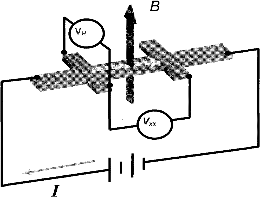
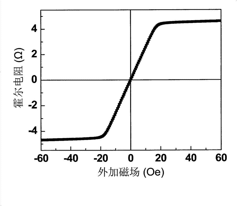
[0022] figure 1 It is a schematic diagram of the structure of the Hall resistance strip. figure 2 It is the Hall signal output curve of this film material measured by the standard four-probe met...
Embodiment 2
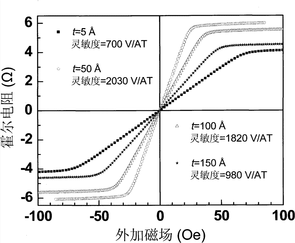
[0024] Magnetic thin films were prepared in a magnetron sputtering apparatus. First, the single crystal silicon substrate is ultrasonically cleaned with an organic chemical solvent and deionized water, and then placed on a sample base in a vacuum sputtering chamber. The substrate is cooled with circulating water. Background vacuum 1×10 during sputtering -5 Pa, the deposition structure is (t takes 5 respectively, ) series of films. Then, the thin film material is processed into a Hall resistance bar element with a line width of 30 microns through the general semiconductor processing technology; the general semiconductor processing technology refers to: glue removal, exposure, development, film hardening, etching, etc.
[0025] image 3 It is a series of thin film materials with the above structure designed and processed into the Hall signal output curve of the Hall resistance strip element; it can be seen that by optimizing the thickness of the insulating layer, Hall sen...
Embodiment 3
[0027] Magnetic thin films were prepared in a magnetron sputtering apparatus. First, the single crystal silicon substrate is ultrasonically cleaned with an organic chemical solvent and deionized water, and then placed on a sample base in a vacuum sputtering chamber. The substrate is cooled with circulating water. Background vacuum 1×10 during sputtering -5 Pa, the deposition structure is (n takes 2-10) and the structure is (n takes 2-10) series of films. Then, the thin film material is processed into a Hall resistance bar element with a line width of 30 microns through the general semiconductor processing technology; the general semiconductor processing technology refers to: glue removal, exposure, development, film hardening, etching, etc.
[0028] Figure 4 It is a series of thin film materials with the above structure designed and processed into a curve of the magnetic field sensitivity of the Hall resistance bar element changing with the number of cycles n. It ...
PUM
 Abstract
Description
Claims
Application Information
 - R&D
- Intellectual Property
- Life Sciences
- Materials
- Tech Scout
- Unparalleled Data Quality
- Higher Quality Content
- 60% Fewer Hallucinations
Browse by: Latest US Patents, China's latest patents, Technical Efficacy Thesaurus, Application Domain, Technology Topic, Popular Technical Reports.
© 2025 PatSnap. All rights reserved.Legal|Privacy policy|Modern Slavery Act Transparency Statement|Sitemap|About US| Contact US: help@patsnap.com


