

Plasma display screen
A plasma and display screen technology, applied in solid cathode components, cold cathode tubes, etc., can solve the problems of low discharge efficiency, low utilization rate of effective area in pixels, etc., and achieves common materials, simple device structure and preparation process, The effect of low process cost
- Summary
- Abstract
- Description
- Claims
- Application Information
AI Technical Summary
Problems solved by technology
Method used
Image

Examples
Embodiment 1
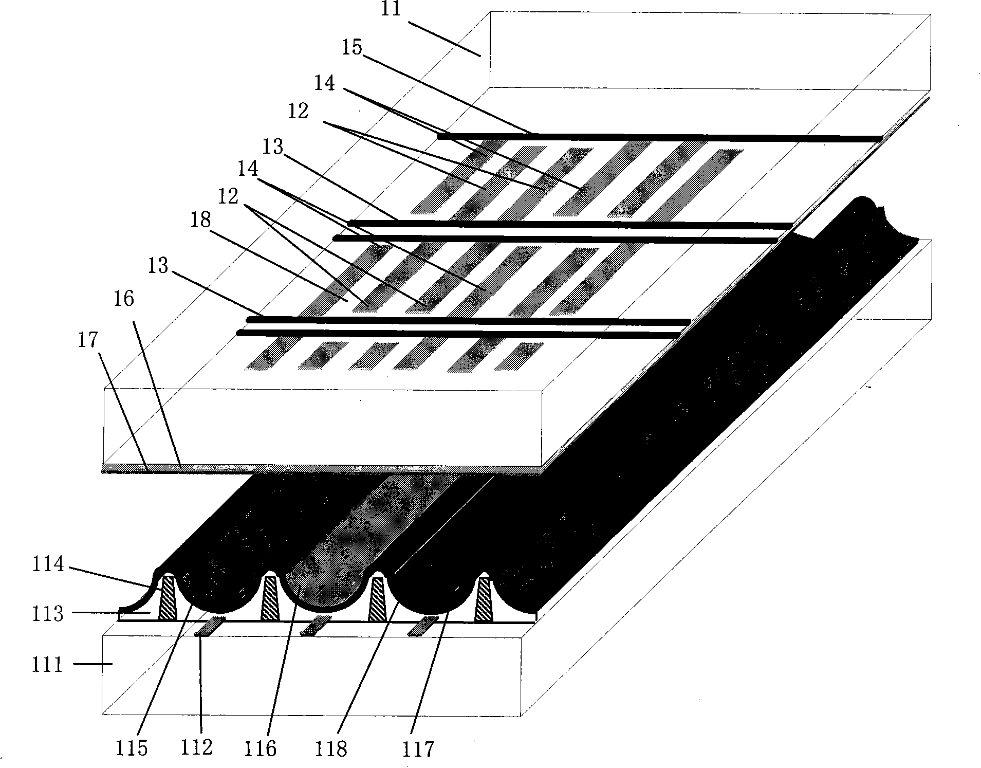
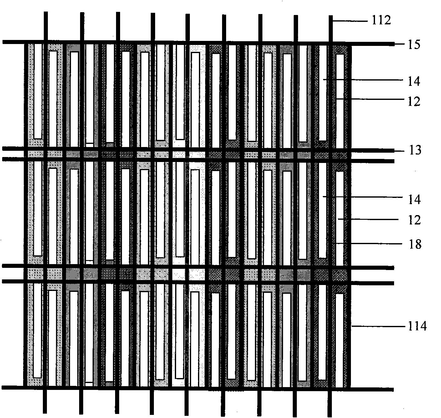
[0027] Such as figure 1 The shown 42-inch high-definition display screen has 1920×1080 pixels, and the sub-pixel size is 160 μm×480 μm. The A electrode is prepared by conventional screen printing on the rear plate glass, the barrier and the rear plate dielectric layer are prepared by screen printing and sintering process, and the three primary color phosphors are coated by the screen printing method. The transparent and conductive X electrodes and Y electrodes on the front panel are rectangular double-finger structures, which are prepared by standard photolithography and etching techniques. The width of the X electrodes and Y electrodes is 30 μm, and the gap width between them is 60 μm. is 200 μm; the bus electrodes of the X electrode and the Y electrode are prepared by screen printing technology, each width is 30 μm, and the distance between them is 160 μm. The dielectric layer of the front plate was prepared by screen printing technology, and the dielectric protection layer...
Embodiment 2
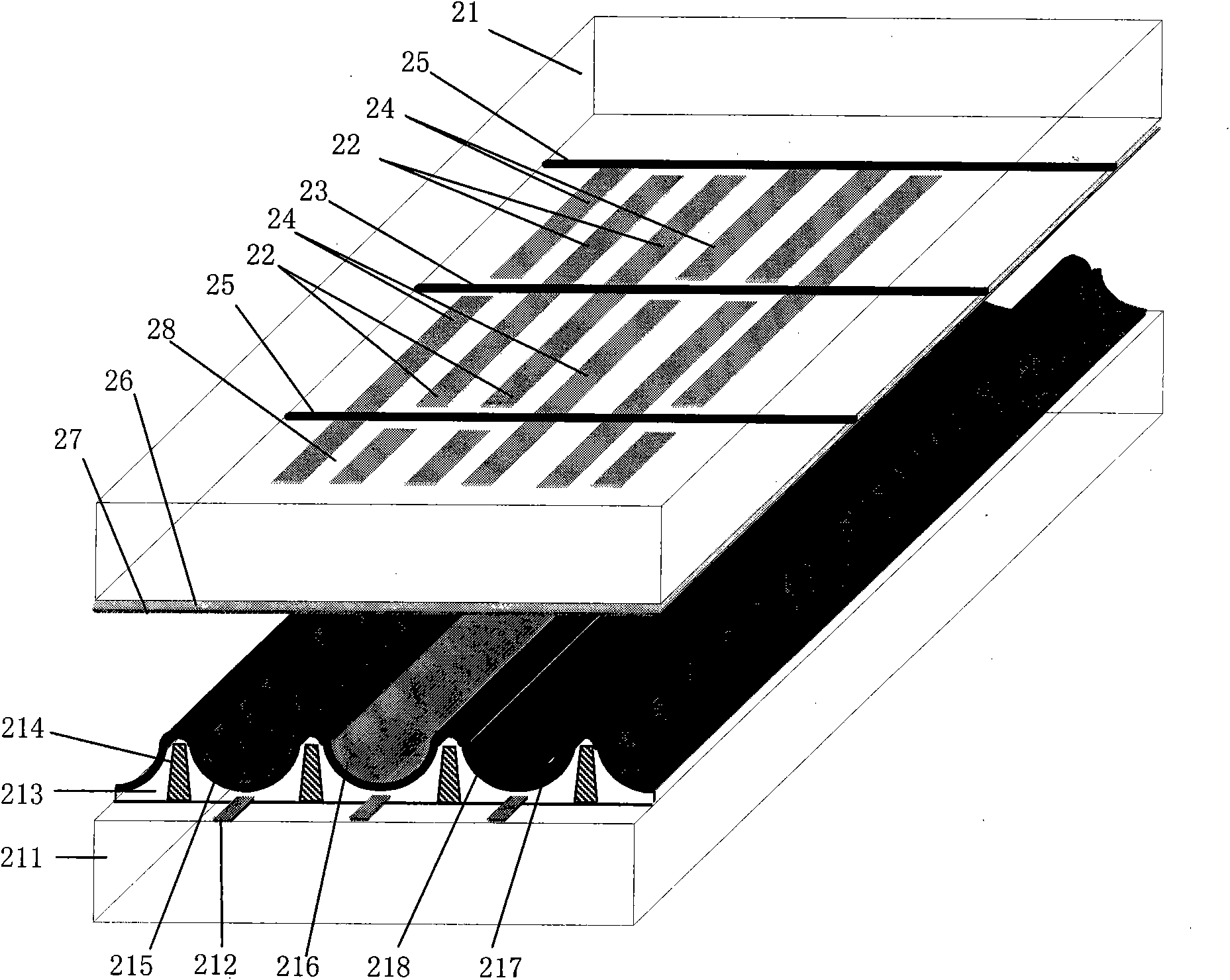
[0029] Such as figure 2 The shown 42-inch high-definition display screen has 1920×1080 pixels, and the sub-pixel size is 160 μm×480 μm. The A electrode is prepared by conventional screen printing on the rear plate glass, the barrier and the rear plate dielectric layer are prepared by screen printing and sintering process, and the three primary color phosphors are coated by the screen printing method. The transparent and conductive X electrodes and Y electrodes on the front panel are rectangular double-finger structures, which are prepared by standard photolithography and etching techniques. The width of the X electrodes and Y electrodes is 30 μm, and the gap width between them is 60 μm. is 360 μm; the bus electrodes of the X electrode and the Y electrode are prepared by screen printing technology, and the width is 30 μm each. The dielectric layer of the front plate was prepared by screen printing technology, and the dielectric protection layer of magnesium oxide with a thick...
Embodiment 3
[0031] Such as image 3 The shown 42-inch high-definition display screen has 1920×1080 pixels, and the sub-pixel size is 160 μm×480 μm. The A electrode is prepared by conventional screen printing on the rear plate glass, the barrier and the rear plate dielectric layer are prepared by screen printing and sintering process, and the three primary color phosphors are coated by the screen printing method. The transparent and conductive X electrodes and Y electrodes on the front plate are rectangular interfinger structures, prepared by standard photolithography and etching techniques, the width of the X electrodes and the Y electrodes is 100 μm, the gap width between them is 60 μm, and the gap length is 200 μm; the bus electrodes of X electrodes and Y electrodes are prepared by screen printing technology, each width is 30 μm, and the distance between them is 160 μm. The dielectric layer of the front plate was prepared by screen printing technology, and the dielectric protection lay...
PUM
 Abstract
Description
Claims
Application Information