GaN-based light-emitting diode epitaxial wafer and growing method thereof

A technology of light-emitting diodes and growth methods, applied in the field of GaN-based light-emitting diode epitaxial wafers and their growth, can solve problems such as high difficulty, long-term stable production instability, and complex growth, and achieve the effects of reducing density and improving ESD resistance

Inactive Publication Date: 2011-05-04
DALIAN MEIMING EPITAXIAL WAFER TECH
View PDF4 Cites 16 Cited by
  • Summary
  • Abstract
  • Description
  • Claims
  • Application Information

AI Technical Summary

Problems solved by technology

The patent "An epitaxial growth method for improving the antistatic ability of gallium nitride-based LED chips" (application number 200710051864.6) mentions that P-type AlGaN and P-type GaN are grown after growing multiple quantum wells, which is characterized in that P-type AlGaN and P-type GaN Small and evenly distributed free metal droplets are formed between P-type GaN to form current release channels to improve the antistatic ability of epitaxial wafers; however, the growth of the above two methods is relatively complicated and difficult, and contains Al components during the growth process , for large-scale production, it is difficult to remove Al by high-temperature baking after growth, which is an unstable factor for long-term stable production

Method used


Image

  • GaN-based light-emitting diode epitaxial wafer and growing method thereof
  • GaN-based light-emitting diode epitaxial wafer and growing method thereof

Examples


Embodiment 1

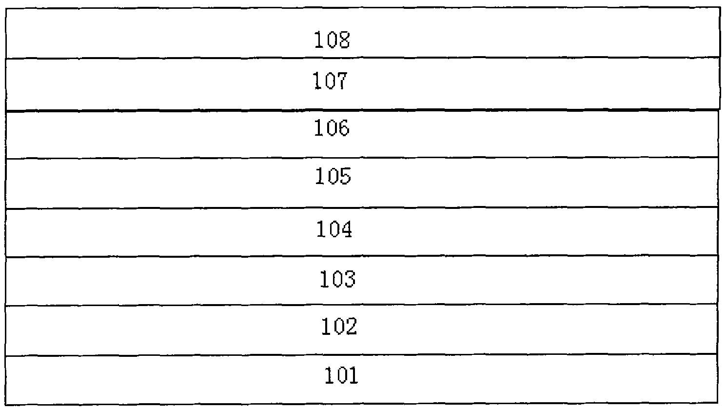
[0012] The MOCVD method is used to grow sequentially from bottom to top:

[0013] 1. Put the sapphire substrate with (0001) crystal orientation into the reaction chamber, and then 2 The temperature in the environment is raised to 1100° C., stabilized for 3 minutes, and the substrate is purified at high temperature.

[0014] 2. Lower the temperature to 530° C. and grow a low-temperature gallium nitride-based buffer layer with a thickness of 20 nm at a growth pressure of 300 mbar.

[0015] 3. The temperature is raised to 1170° C., the growth pressure is 100 mbar, and non-doped gallium nitride with a thickness of 1.3 μm is grown.

[0016] 4. At 1170° C. and a growth pressure of 100 mbar, grow n-type gallium nitride with a thickness of 1.5 μm.

[0017] 5. In N 2 The multi-quantum well layer is grown for 5 cycles in the environment, the growth pressure is 100mbar, the GaN barrier layer: the thickness is 10nm, the growth temperature is 800°C; the InGaN well layer: the thickness i...

Embodiment 2

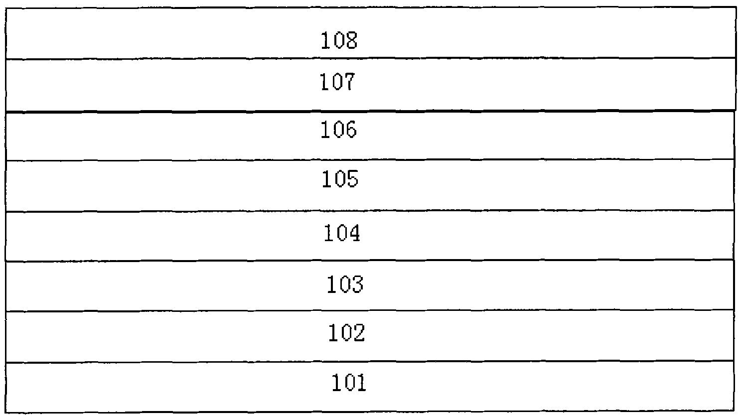
[0024] The MOCVD method is used to grow sequentially from bottom to top:

[0025] 1. Put the sapphire substrate with (0001) crystal orientation into the reaction chamber, and then 2 The temperature in the environment is raised to 1200° C., stabilized for 5 minutes, and the substrate is purified at high temperature.

[0026] 2. Lower the temperature to 550° C. and grow a low-temperature gallium nitride-based buffer layer with a thickness of 40 nm at a growth pressure of 500 mbar.

[0027] 3. Raise the temperature to 1180° C. and grow the non-doped GaN with a thickness of 1.5 μm at a growth pressure of 300 mbar.

[0028] 4. At 1180° C. and a growth pressure of 300 mbar, grow n-type gallium nitride with a thickness of 1.7 μm.

[0029] 5. In N 2 The multi-quantum well layer is grown for 5 cycles in the environment, the growth pressure is 100mbar, the GaN barrier layer: the thickness is 10nm, the growth temperature is 800°C; the InGaN well layer: the thickness is 1nm, the growth...

Embodiment 3

[0036] The MOCVD method is used to grow sequentially from bottom to top:

[0037] 1. Put the sapphire substrate with (0001) crystal orientation into the reaction chamber, and then 2 The temperature in the environment is raised to 1200° C., stabilized for 5 minutes, and the substrate is purified at high temperature.

[0038] 2. Lower the temperature to 570° C. and grow a low-temperature gallium nitride-based buffer layer with a thickness of 50 nm at a growth pressure of 700 mbar.

[0039] 3. Raise the temperature to 1190° C. and grow the non-doped GaN with a thickness of 1.8 μm at a growth pressure of 700 mbar.

[0040] 4. At 1190° C. and a growth pressure of 700 mbar, grow n-type gallium nitride with a thickness of 2 μm.

[0041] 5. In N 2 The multi-quantum well layer is grown for 5 cycles in the environment, the growth pressure is 100mbar, the GaN barrier layer: the thickness is 10nm, the growth temperature is 800°C; the InGaN well layer: the thickness is 1nm, the growth tem...


PUM


Abstract

The invention relates to an LED (Light-Emitting Diode) epitaxial wafer and a growing method thereof, wherein the LED epitaxial wafer comprises two p-type GaN layers, and the growing method of the LED epitaxial wafer comprises the following steps of: when the p-type GaN layers grow, firstly growing a first p-type GaN layer at lower temperature and under lower pressure, and then growing a second p-type GaN layer when the temperature is relatively higher. Because the growing temperature of the first p-type GaN layer is low, an irregular structure is formed behind a quantum well to enable static electricity to be easily dispersed, so that the anti-ESD (Electro-Static discharge) capability of a GaN-based LED chip is improved. The invention has the advantages that the anti-ESD capability of the GaN-based LED chip is improved, the 2000V ESD passing rate of the chip with the size of 300*300mu m<2> can reach 98 percent, and the 4000V ESD passing rate can reach 95 percent.

Description

technical field [0001] The invention belongs to the technical field of semiconductors, and relates to an LED epitaxial wafer and an epitaxial growth method thereof, in particular to a GaN-based light-emitting diode epitaxial wafer and a growth method thereof. technical background [0002] At present, the mainstream of blue-green light-emitting diodes is to grow GaN materials on sapphire or silicon carbide substrates, most of which use sapphire as the substrate. Due to the large lattice mismatch and thermal mismatch between the sapphire substrate and the GaN material, high-density defects, such as threading dislocations, are generated in the GaN epitaxial layer. Experiments demonstrate that these defects are an important pathway for reverse leakage current generation in III-nitride-based light-emitting diodes. [0003] The usual practice is to grow a thin low-temperature buffer layer (nucleation layer, Nucleation layer) on the sapphire first, and then people optimize the hig...

Claims


Application Information

Patent Timeline
Patent Type & Authority Applications(China)
IPC IPC(8): H01L33/00
Inventor 芦玲郭文平杨天鹏陈向东肖志国
Owner DALIAN MEIMING EPITAXIAL WAFER TECH
Why Eureka
Try Eureka