LED (Light-Emitting Diode) epitaxial wafer and epitaxial growth method thereof

An LED epitaxial wafer and regrowth technology, applied in electrical components, circuits, semiconductor devices, etc., can solve the problems of reduced number of holes, low activation efficiency, low injection ratio, etc., and achieve the effect of improving brightness

Inactive Publication Date: 2011-05-04
DALIAN MEIMING EPITAXIAL WAFER TECH
View PDF6 Cites 12 Cited by
  • Summary
  • Abstract
  • Description
  • Claims
  • Application Information

AI Technical Summary

Problems solved by technology

However, this structure also has disadvantages: due to the increase of the multi-quantum well buffer layer, and the multi-quantum well doping with Si, n-type impurities are introduced, which makes the P-N junction deviate from the InGaN/GaN multi-quantum well region, and the light-emitting diode works in the forward direction. When the bias voltage is applied, the minority carriers in the quantum well region are holes, and the holes recombine with electrons to emit light during the diffusion process. However, due to the low mobility of the holes and the small d

Method used


Image

  • LED (Light-Emitting Diode) epitaxial wafer and epitaxial growth method thereof
  • LED (Light-Emitting Diode) epitaxial wafer and epitaxial growth method thereof
  • LED (Light-Emitting Diode) epitaxial wafer and epitaxial growth method thereof

Examples


Embodiment 1

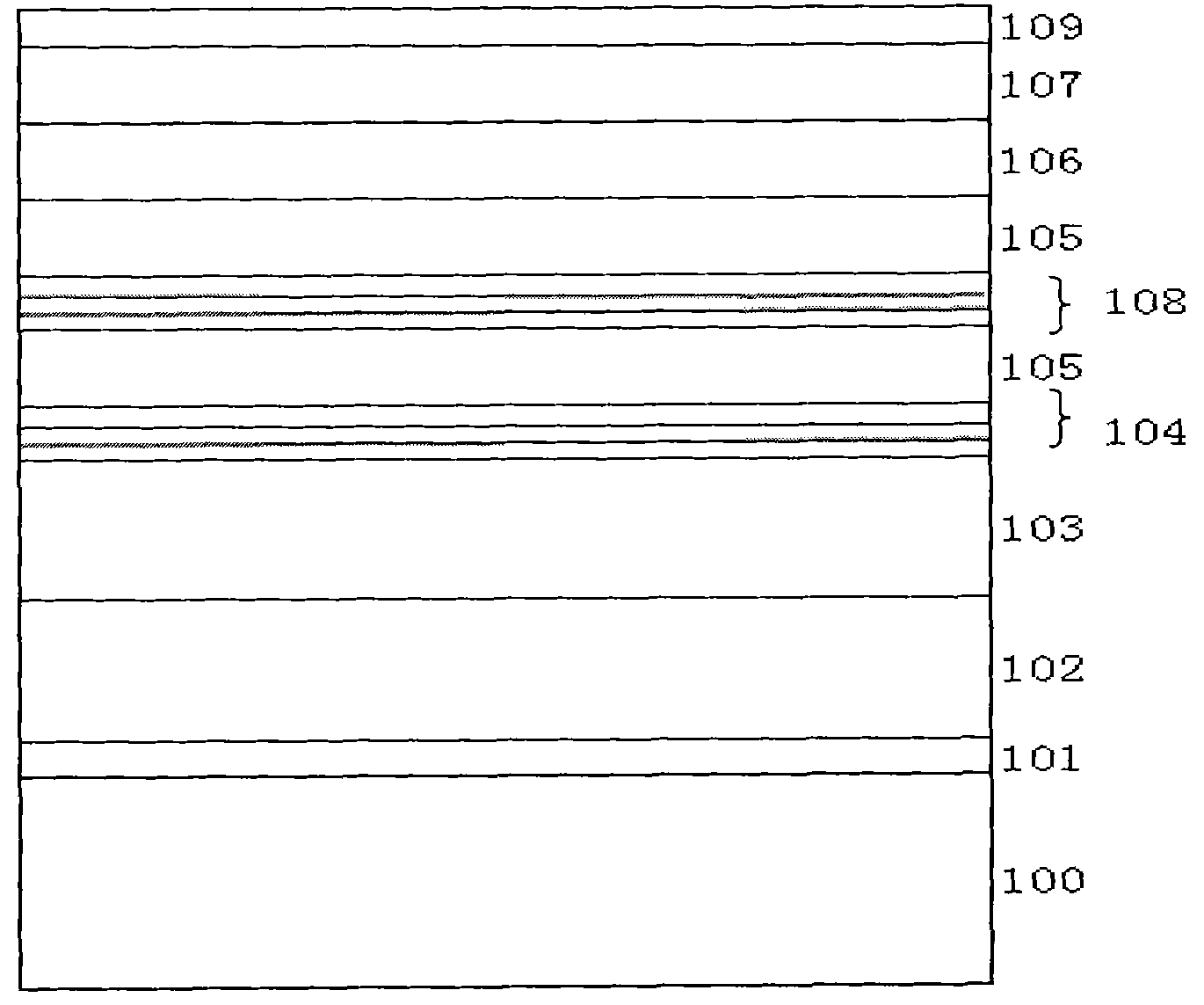
[0041] Embodiment 1 uses MOCVD to grow epitaxial wafers, and grows sequentially from bottom to top:

[0042] 1. Put the sapphire substrate with (0001) crystal orientation into the reaction chamber, and then 2 The temperature in the environment is raised to 1100° C., stabilized for 5 minutes, and the substrate is purified at high temperature.

[0043] 2. Lower the temperature to 500° C. to grow a low-temperature GaN-based buffer layer with a thickness of 20 nm.

[0044] 3. Raise the temperature to 1050° C., and grow a non-doped gallium nitride layer with a thickness of 1 μm.

[0045] 4. At 1100° C., grow an n-type doped gallium nitride layer with a thickness of 2 μm.

[0046] 5. In N 2 5 cycles of multiple quantum well layers were grown in the environment, GaN barrier layer: thickness 22nm, growth temperature 900°C; InGaN well layer: thickness 1.3nm, growth temperature 750°C.

[0047] 6. Raise the temperature to 1000° C. to grow p-type gallium nitride with a thickness of 50...

Embodiment 2

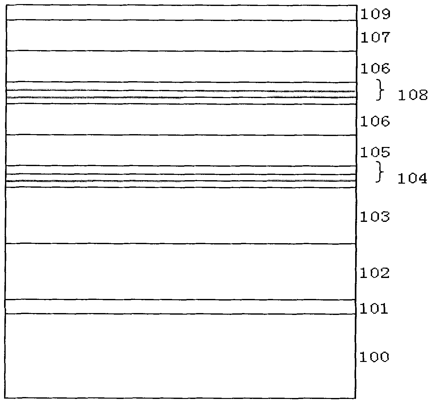
[0056] Embodiment 2 uses MOCVD to grow epitaxial wafers, and grows sequentially from bottom to top:

[0057] 1. Put the sapphire substrate with (0001) crystal orientation into the reaction chamber, and then 2 The temperature in the environment is raised to 1250° C., stabilized for 6 minutes, and the substrate is purified at high temperature.

[0058] 2. Lower the temperature to 550° C. to grow a low-temperature GaN-based buffer layer with a thickness of 40 nm.

[0059] 3. Raise the temperature to 1070° C., and grow a non-doped GaN layer with a thickness of 1 μm.

[0060] 4. At 1050° C., grow an n-type doped gallium nitride layer with a thickness of 3 μm.

[0061] 5. In N 2 The multi-quantum well layer was grown for 10 cycles in the environment, the GaN barrier layer: the thickness was 20nm, and the growth temperature was 850°C; the InGaN well layer: the thickness was 1.0nm, and the growth temperature was 750°C.

[0062] 6. Raise the temperature to 1000° C. to grow p-type g...

Embodiment 3

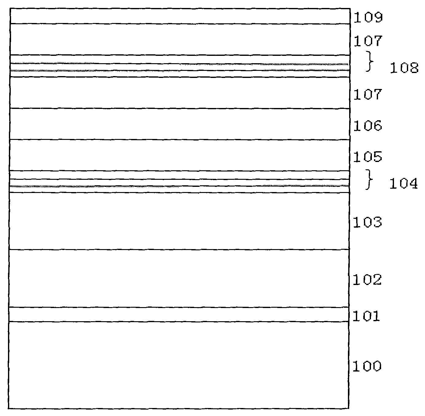
[0071] Embodiment 3 uses MOCVD to grow epitaxial wafers, and grows sequentially from bottom to top:

[0072] 1. Put the sapphire substrate with (0001) crystal orientation into the reaction chamber, and then 2 The temperature in the environment is raised to 1050° C., stabilized for 6 minutes, and the substrate is purified at high temperature.

[0073] 2. Lower the temperature to 550° C. to grow a low-temperature GaN-based buffer layer with a thickness of 30 nm.

[0074] 3. Raise the temperature to 1200° C., and grow a non-doped GaN layer with a thickness of 1 μm.

[0075] 4. At 1050° C., grow an n-type doped gallium nitride layer with a thickness of 3 μm.

[0076] 5. In N 2 8 cycles of multi-quantum well layers are grown in the environment, GaN barrier layer: thickness is 20nm, growth temperature is 850°C; InGaN well layer: thickness is 1.5nm, growth temperature is 740°C.

[0077] 6. Raise the temperature to 800° C. to grow p-type gallium nitride (p1) with a thickness of 10...


PUM

PropertyMeasurementUnit
Thicknessaaaaaaaaaa
Thicknessaaaaaaaaaa
Total thicknessaaaaaaaaaa

Abstract

The invention relates to an LED epitaxial wafer which structurally comprises a sapphire substrate, a low-temperature gallium nitride-based buffer layer, an undoped gallium nitride layer, an n-type gallium nitride layer, multiple quantum wells, a p-type gallium nitride layer, a p-type aluminum gallium nitride layer, a coarsened p-type gallium nitride layer and an expanded current layer in sequence from the bottom up, wherein the expanded current layer can be embedded into the p-type gallium nitride layer or embedded into the p-type aluminum gallium nitride layer or embedded into the coarsened p-type gallium nitride layer. A manufacturing method of the LED epitaxial wafer comprises the step of embedding and growing the expanded current layer into the p-type gallium nitride layer, the p-type aluminum gallium nitride layer or the coarsened p-type gallium nitride layer. Because the forbidden bandwidth of the expanded current layer is smaller, the activation energy of Mg is reduced, the number of cavities entering a light-emitting area is increased, the injection ratio of the cavities in the light-emitting area is improved, and the number of the cavities compounded with electrons for emitting light is increased, thereby the illumination intensity of an LED is improved.

Description

technical field [0001] The invention belongs to the technical field of semiconductors, and relates to an LED epitaxial wafer and an epitaxial growth method thereof, in particular to an LED epitaxial wafer embedded with an expansion current layer during the growth process of p-type gallium nitride and an epitaxial growth method thereof. technical background [0002] The application of LED is more and more extensive, mainly used in LCD screen backlight, LED lighting, LED display. The application of commercial products such as blue light-emitting diodes and green light-emitting diodes (LEDs) all illustrate the hidden potential of III-V elements. In the past ten years, in order to develop high-brightness light-emitting diodes, relevant research personnel all over the world have devoted themselves to it, but the problem of low luminous intensity still exists. Reducing the thermal resistance of devices and systems, thereby lowering the temperature; optimizing the LED epitaxial st...

Claims


Application Information

Patent Timeline
IPC IPC(8): H01L33/14
Inventor 吴雪花杨天鹏郭文平陈向东肖志国
Owner DALIAN MEIMING EPITAXIAL WAFER TECH
Why Eureka
Try Eureka