Dicing method

A cutting method and chip technology, applied in adhesive types, film/sheet adhesives, polyurea/polyurethane adhesives, etc., can solve the difficulty of chip peeling, increase the difficulty of chip picking, and pick up Defects and other problems can be achieved to reduce the phenomenon of mixing and suppress the effect of chip pick-up defects

Active Publication Date: 2011-05-04
DENKA CO LTD
View PDF2 Cites 2 Cited by
  • Summary
  • Abstract
  • Description
  • Claims
  • Application Information

AI Technical Summary

Problems solved by technology

[0006] However, with the high integration of semiconductor components, the size of the chip increases and the thickness becomes smaller, which increases the difficulty of picking up the chip after dicing
[0007] Moreover, since not only the semiconductor wafer but also the adhesive layer of the die attach film and the adhesive sheet are cut at the time of dicing, the die attach film and the adhesive layer tend to be mixed at the dicing line, Even if the adhesive strength is sufficiently reduced by irradiating ultraviolet light after dicing, it is difficult to peel off the chip when picking it up, which may cause pick-up failure

Method used


Image

  • Dicing method
  • Dicing method

Examples


preparation example Construction

[0045] As a method for producing the (meth)acrylate polymer, emulsion polymerization, solution polymerization, or the like can be used. The (meth)acrylate polymer is preferably an acrylic rubber prepared by emulsion polymerization in consideration of pick-up property.

[0046] Examples of the rubber-based adhesive include natural rubber, synthetic isoprene rubber, styrene-butadiene rubber, styrene-butadiene block copolymer, styrene-isoprene block copolymer, Butyl rubber, polyisobutylene, polybutadiene, polyvinyl ether, silicone rubber, polyvinyl isobutyl ether, neoprene, nitrile rubber, craft rubber, recycled rubber, styrene vinyl ・Butene block copolymer, styrene-propylene-butylene block copolymer, styrene-isoprene block copolymer, polyisobutylene-ethylene-propylene copolymer, ethylene-vinyl acetate copolymer, polyisobutylene ・Silicone rubber, polyvinyl isobutyl ether, chloroprene, etc. The aforementioned rubber-based adhesive may be one of them or a mixture thereof.

[0047]...

Embodiment

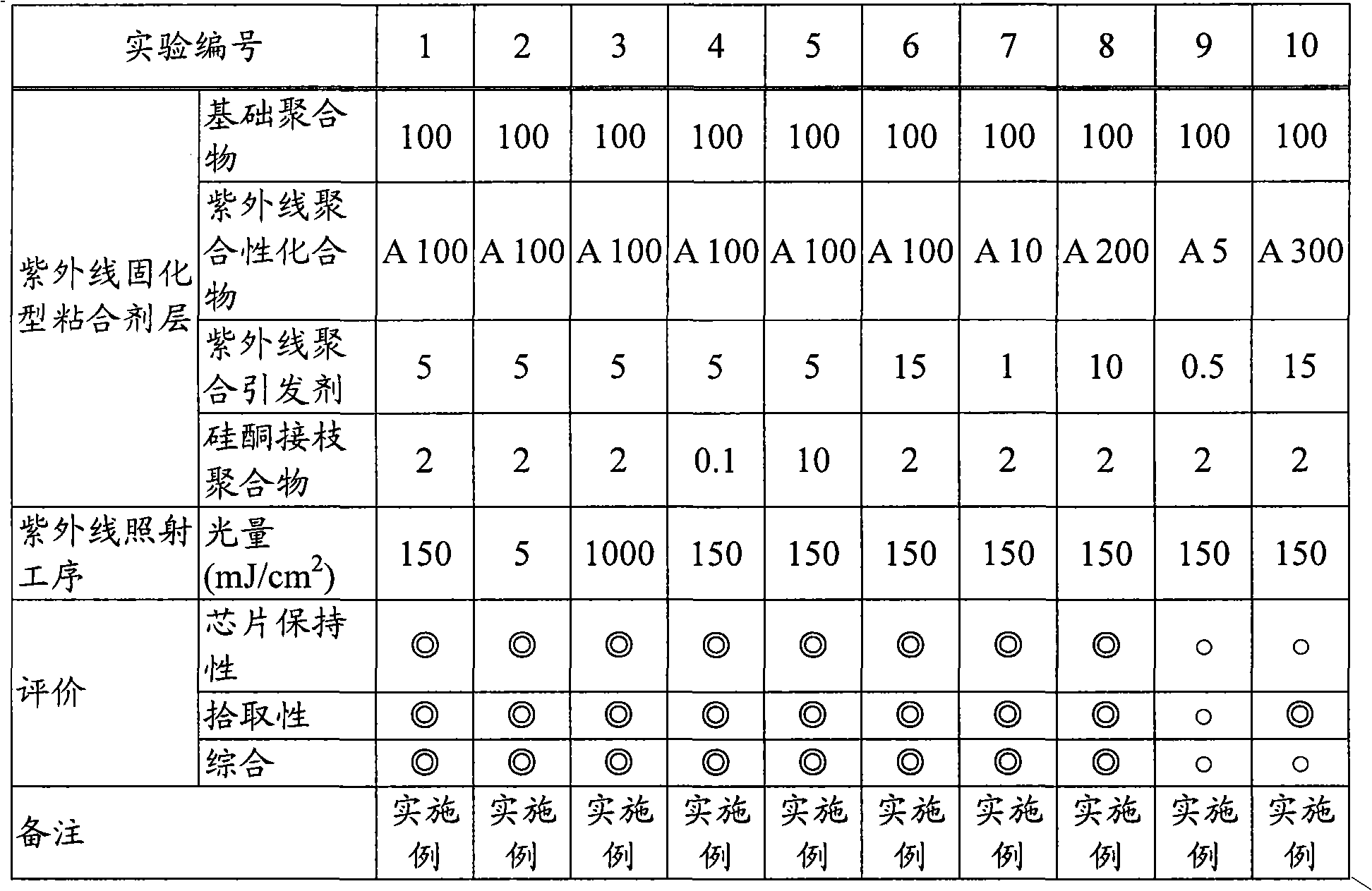
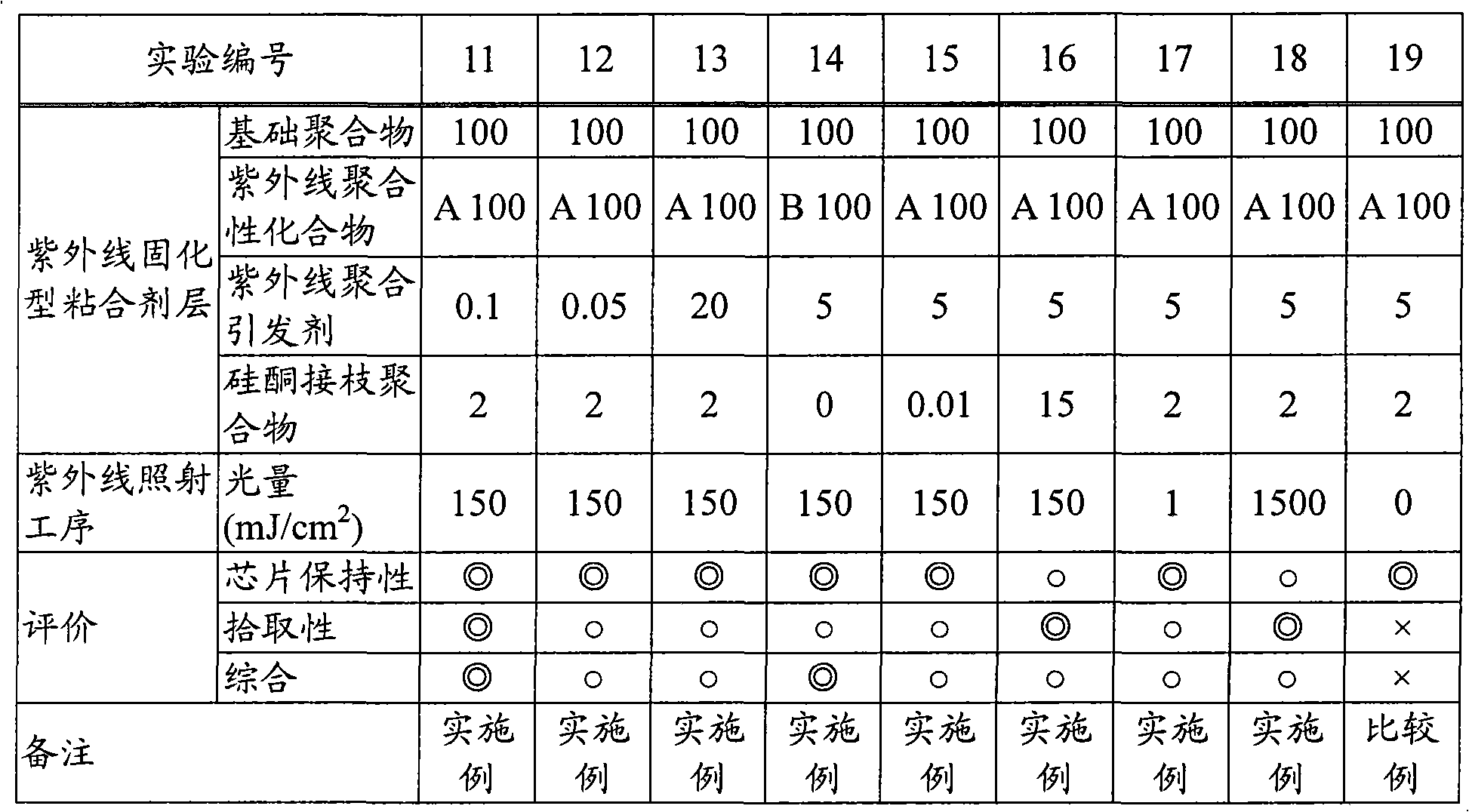
[0094] Hereinafter, the present invention will be further described through examples, but the present invention is not limited to the following examples.


PUM

PropertyMeasurementUnit
thicknessaaaaaaaaaa
thicknessaaaaaaaaaa
thicknessaaaaaaaaaa

Abstract

With the invented dicing method, by increasing the cohesive strength while decreasing the adhesive strength of an ultraviolet-curing adhesive in advance, mixing of the ultraviolet-curing adhesive layer of an adhesive sheet with a die attach film on a dicing line can be decreased and pickup failures can be reduced, when picking up chips having a die attach film after dicing. The dicing method for a semiconductor wafer with a die-attach film comprises a first gluing step in which a die attach film is affixed to an adhesive sheet having an ultraviolet-curing adhesive laminated on a base materialfilm, a second gluing step in which a semiconductor wafer is affixed to the opposite side of the die attach film affixed to the adhesive sheet, an ultraviolet irradiation step in which the ultraviolet-curing adhesive is irradiated with ultraviolet light, and a dicing step in which the semiconductor wafer and the die attach film affixed to the adhesive sheet are diced.

Description

technical field [0001] The present invention relates to a dicing method for dicing a semiconductor wafer with a die attach film into chips. Background technique [0002] One of the manufacturing methods of electronic components includes: a bonding process of bonding an electronic component assembly or wafer composed of a plurality of circuit patterns formed on an insulating substrate to an adhesive sheet; a cutting / separating process (dicing process), The bonded wafer or electronic component assembly is cut to form chips; the ultraviolet irradiation process, after the cutting process, irradiates ultraviolet rays from the side of the adhesive sheet to reduce the adhesive force of the adhesive layer; the pick-up process, from Pick up each of the above-cut chips on the adhesive sheet; the fixing process, after coating the bottom surface of the picked-up chip with an adhesive, fix the chip to a lead frame or the like through the adhesive. [0003] There is also a method in whic...

Claims


Application Information

Patent Timeline
Patent Type & Authority Applications(China)
IPC IPC(8): H01L21/301C09J11/06C09J133/06C09J175/16C09J183/10H01L21/52C09J7/02
CPCC08G18/10C08G18/6229C08G18/672C08G18/673C08G18/73C08G18/792C09D183/10H01L21/67132H01L21/6836H01L24/27H01L24/29H01L24/83H01L2221/68327H01L2224/27436H01L2224/2919H01L2224/83191H01L2224/8385H01L2924/01005H01L2924/01006H01L2924/01011H01L2924/01015H01L2924/01019H01L2924/01025H01L2924/0103H01L2924/01033H01L2924/01075H01L2924/01082H01L2924/0665H01L2924/07802C08G18/61H01L2924/00
Inventor 齐藤岳史高津知道
Owner DENKA CO LTD
Why Eureka
Try Eureka