Method for measuring thermal conductivity of single semiconductor nanowire material

A nanowire and semiconductor technology, applied in the field of thermal conductivity measurement of a single semiconductor nanowire material, can solve the problems of expensive microfabrication equipment, influence of thermal conductivity of samples, complicated and tedious manufacturing process of microstructure devices, etc., to avoid damage, The effect of saving resources

Active Publication Date: 2011-05-11
THE NAT CENT FOR NANOSCI & TECH NCNST OF CHINA
View PDF0 Cites 13 Cited by
  • Summary
  • Abstract
  • Description
  • Claims
  • Application Information

AI Technical Summary

Problems solved by technology

[0004] The disadvantage of the above micro-device method is that electrodes need to be overlapped at both ends of the sample, which can have a great impact on the thermal conduc

Method used


Image

  • Method for measuring thermal conductivity of single semiconductor nanowire material
  • Method for measuring thermal conductivity of single semiconductor nanowire material
  • Method for measuring thermal conductivity of single semiconductor nanowire material

Examples


Embodiment 1

[0040] In this embodiment, the method of the present invention is used to measure the thermal conductivity of a single semiconductor CdS nanowire, and the specific steps are as follows:

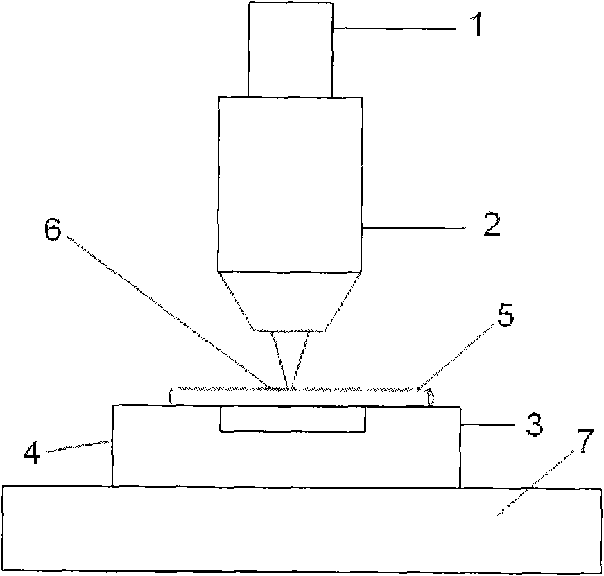
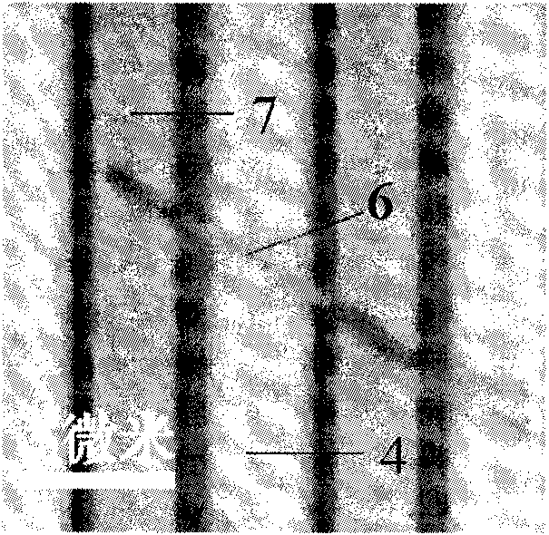
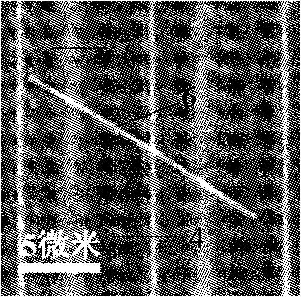
[0041] Step 1. Utilize the FIB technology to etch a group of (5 grooves) grooves 4 on the surface of the cleaned silicon substrate 3, the width of the grooves 4 is 5 microns, the length is 100 microns, and the depth is 0.8 microns; The cross-sectional shape of the groove 4 is rectangular; the purpose of etching the groove is to generate a local temperature when the laser is focused on the suspended part of the nanowire;

[0042] Step 2. Obtain a single CdS nanowire 6 suspended above the groove 4 by spin-coating an alcohol solution of the CdS nanowire. In order to improve the efficiency of hanging on the groove, the microprobe operation method can also be used to directly manipulate a single semiconductor CdS nanowire 6 and place it on the Si substrate groove 4; see Figure 2a , showing an op...

Embodiment 2

[0056] For the measurement of the thermal conductivity of a single ZnO nanowire, the measurement method and steps in this example are the same as those in Example 1. In this embodiment, the difference from Embodiment 1 is:

[0057] The substrate is an ITO substrate etched with grooves.

[0058] The cross-section of the groove is semicircular, the number of grooves is 10, the width of the groove is 6 microns, the depth of the groove is 0.5 microns, and the length of the grooves is 100 microns.

[0059] Described excitation light source is the 325nm laser that can excite ZnO band edge fluorescence, and the diameter of laser spot (D 2 =2) microns, the laser energy distribution is Gaussian distribution.

[0060] The size of the ZnO nanowires, according to electron micrographs nanowire diameter (D 1 = 0.3 microns).

[0061] According to the step in embodiment 1, obtain and calculate every parameter of single ZnO nanowire, namely the diameter (D of ZnO nanowire to be measured) ...

Embodiment 3

[0063] Measuring the thermal conductivity of a single semiconducting ZnS nanowire

[0064] The method and steps of measuring the thermal conductivity of the nanowires in Example 1 are the same, and the thermal conductivity of a single ZnS nanowire is measured. In this embodiment, the difference from Embodiment 1 is:

[0065] The substrate is a gold-plated Si substrate etched with grooves.

[0066] The cross-section of the groove is rectangular, the number of grooves is 2, the width of the groove is 5 microns, the depth of the groove is 0.7 microns, and the length of the grooves is 100 microns.

[0067] Described excitation light source is the 405nm laser that can excite ZnS band edge fluorescence, and the diameter of laser spot (D 2 =2) microns, the laser energy distribution is Gaussian distribution.

[0068] The size of the ZnS nanowires, according to electron micrographs nanowire diameter (D 1 = 0.35 microns).

[0069] According to the step in embodiment 1, obtain and c...


PUM

PropertyMeasurementUnit
Widthaaaaaaaaaa
Lengthaaaaaaaaaa
Widthaaaaaaaaaa

Abstract

The invention relates to a method for measuring the thermal conductivity of a single semiconductor nanowire material. The method comprises the following steps of: suspending a semiconductor nanowire material to be measured on a substrate etched with a groove; confirming the diameter D1 of the semiconductor nanowire to be measured and the length L of the suspended part of the semiconductor nanowire sample suspended on the groove through an SEM (Scanning Electron Microscope); selecting an excitation light source, observing the remarkable red shift of the peak position of a band-edge fluorescence transmitter peak of the nanowire when laser is focused in the center of the suspended part of the nanowire and the laser strength is changed, measuring the variance relation of the nanowire fluorescence spectrum with temperatures and estimating the local temperature of the suspended nanowire part under the laser illumination so as to acquire the temperature grads of the nanowire under a certain laser power density. According to the calculation of a heat conduction equation of a one-dimensional nanowire sample: K=x*(2L/pai*D12)(beta*lambda/beta*pa)-1, the thermal conductivity of a single nanowire is derived. The method for deriving the local temperature and the thermal conductivity by utilizing the photoluminescent property of the semiconductor material is practically applied to the aspect of non-contact micro-nano thermal property measurement.

Description

technical field [0001] The invention belongs to the technical field of measuring thermal conductivity of materials, in particular to a method for measuring the thermal conductivity of a single semiconductor nanowire material. Background technique [0002] The heat conduction behavior of materials has received extensive attention in the fields of thermal power, chemical engineering, electronic devices, construction, aerospace and bioengineering. For example, in microelectronics technology, the cooling of electronic components and the cooling of electronic equipment need to know the heat conduction of materials. properties, that is, the thermal conductivity of the material that needs to be tested. The thermal conductivity of a material is a physical quantity that characterizes the thermal conductivity of a substance, and is one of the important physical parameters of a material. Therefore, it is a subject of practical application significance to explore the measurement method ...

Claims


Application Information

Patent Timeline
IPC IPC(8): G01N25/20
Inventor 刘新风宁廷银裘晓辉
Owner THE NAT CENT FOR NANOSCI & TECH NCNST OF CHINA
Why Eureka
Try Eureka