

Active differential voltage probe
A differential voltage and fully differential amplifier technology, which is applied in the direction of measuring electricity, measuring electrical variables, and components of electrical measuring instruments, etc., can solve the problems of affecting the detection effect of the probe, poor frequency response, impedance mismatch, etc., and achieve the probe frequency response Good, small input capacitance, wide detection bandwidth effect
- Summary
- Abstract
- Description
- Claims
- Application Information
AI Technical Summary
Problems solved by technology
Method used
Image

Examples
Embodiment 1
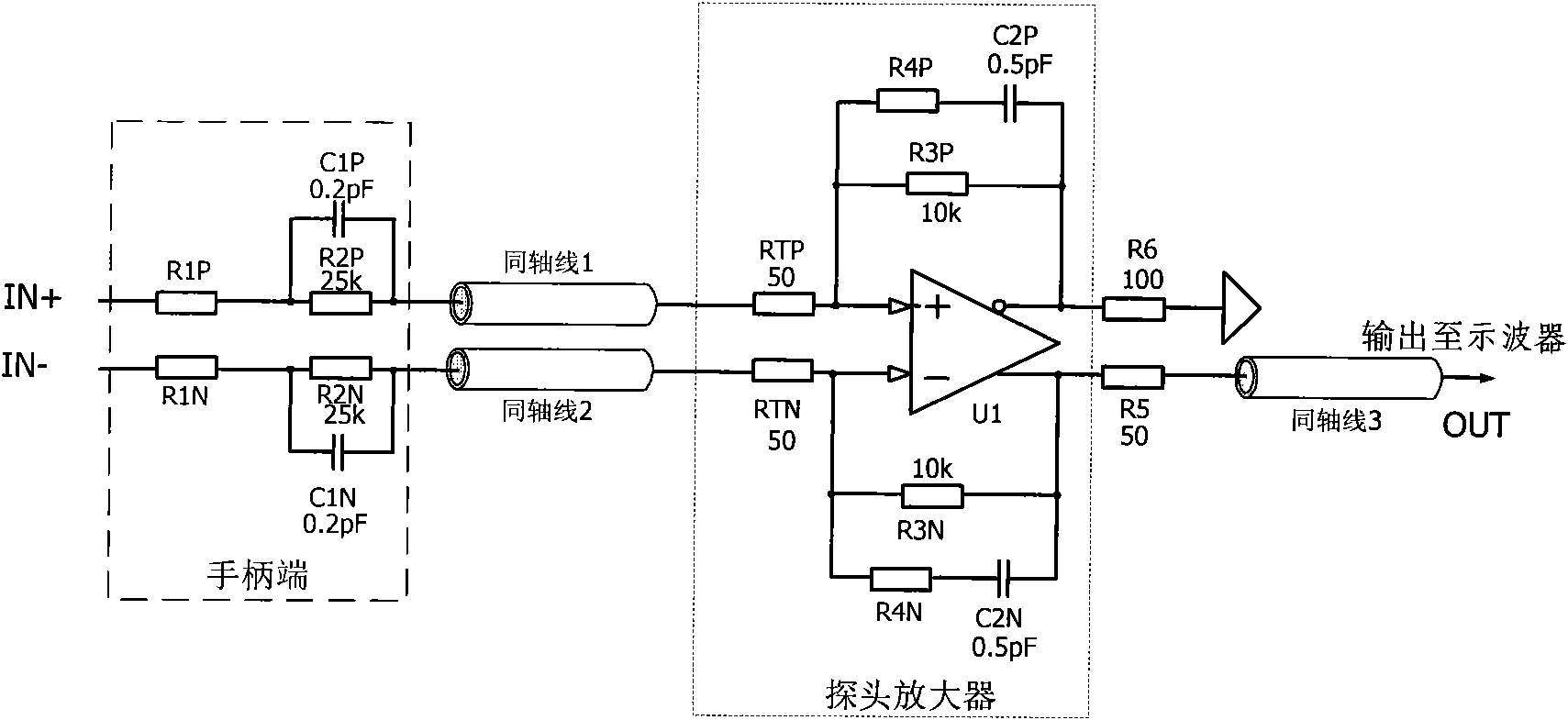
[0028] figure 1 It is the circuit diagram of the first embodiment of the active differential voltage probe. As shown, this active differential voltage probe consists of a handle end, a coaxial cable, and a probe amplifier.
[0029] The handle end is provided with two input terminals IN+ and IN- for measuring the positive and negative terminals of the differential signal. The input terminal IN+ is connected with a damping resistor R1P, and the input terminal IN- is connected with a damping resistor R1N. The damping resistor R1P is connected in series with the RC voltage divider circuit formed by the parallel connection of the resistor R2P and the capacitor C1P. The damping resistor R1N is connected in series with the RC voltage divider circuit formed by parallel connection of the resistor R2N and the capacitor C1N. The other end of the RC voltage divider circuit formed by parallel connection of the resistor R2P and the capacitor C1P is connected to the positive output end o...
Embodiment 2
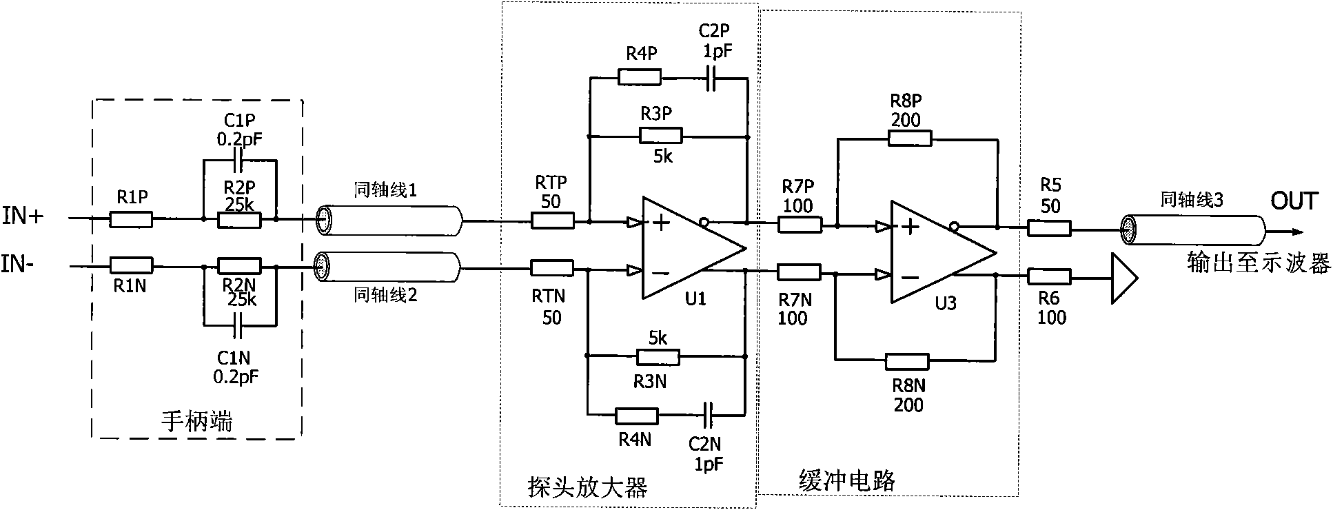
[0041] figure 1 In the first embodiment shown, the active differential voltage probe only uses a fully differential amplifier U1 to implement a proportional amplification circuit. However, if only the one-stage amplifying circuit cannot meet the overall attenuation multiple requirements under the condition of achieving the required bandwidth, the second-stage buffer circuit can be designed to achieve insufficient gain, so as to ensure that the gain of the entire circuit is the gain required by the probe. . figure 2 That is, the circuit diagram of the second embodiment of the active differential voltage probe is given. As shown in the figure, in the second embodiment, a buffer circuit is connected in series between the probe amplifier and the resistors R5 and R6.
[0042] As shown in the figure, the buffer circuit consists of a fully differential amplifier U3 and several resistors. The positive input terminal of the fully differential amplifier U3 is connected to the posit...
Embodiment 3
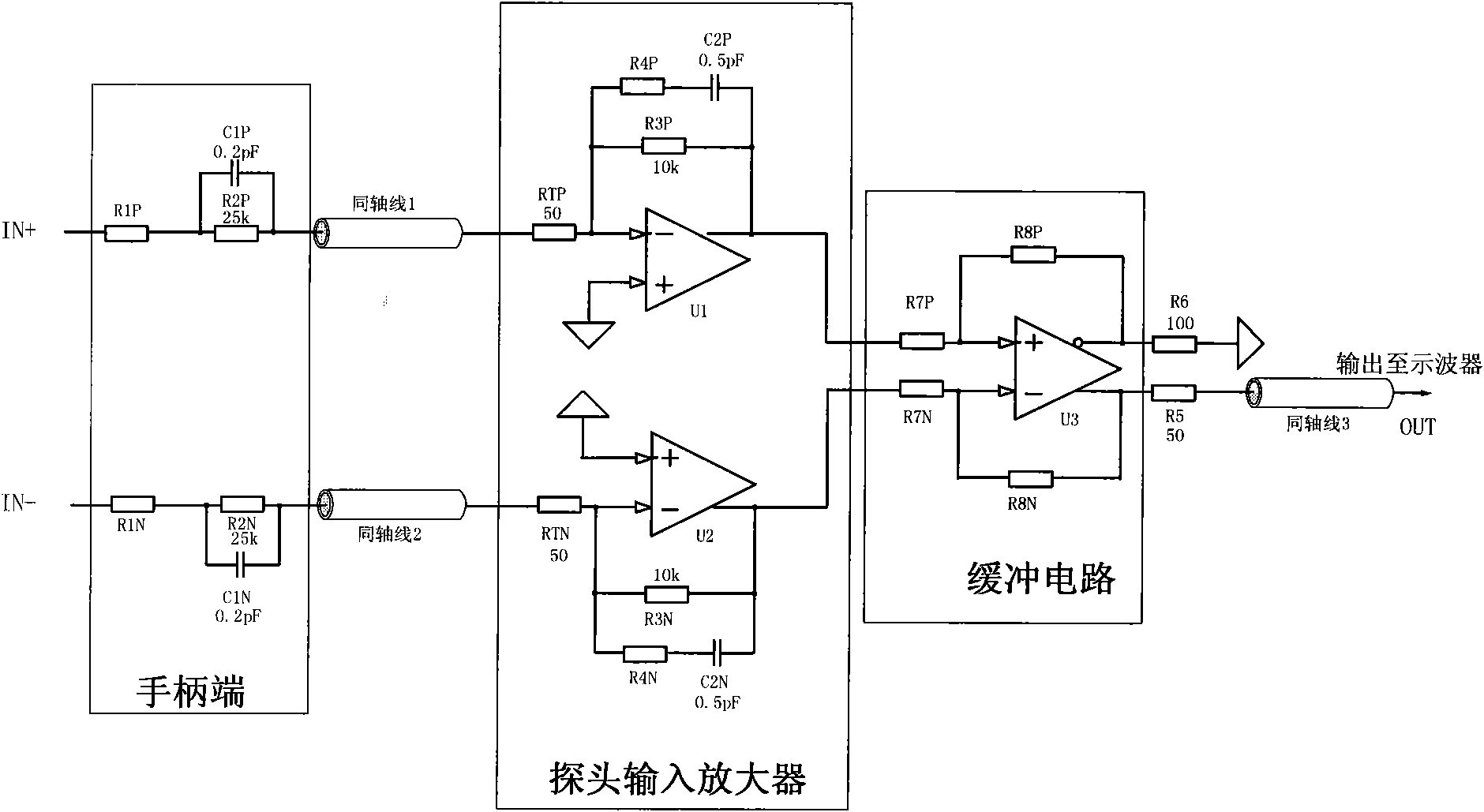
[0046] In addition to the single amplifier design shown in the first embodiment and the second embodiment, the probe amplifier can also adopt the design mode of two amplifiers. image 3 It is the circuit diagram of the third embodiment of the active differential voltage probe.
[0047] As shown in the figure, the probe amplifier consists of a fully differential amplifier U1, a fully differential amplifier U2 and several capacitors and resistors. The positive input end of the probe amplifier is connected with a terminal resistor RTP, and the negative input end of the probe amplifier is connected with a terminal resistor RTN. The terminal resistor RTP is connected to the negative input terminal of the fully differential amplifier U1, and the terminal resistor RTN is connected to the negative input terminal of the fully differential amplifier U2. The positive input terminals of the fully differential amplifiers U1, U2 are grounded. An RC voltage divider circuit composed of a res...
PUM
 Abstract
Description
Claims
Application Information