
Method for improving junction depth property of semiconductor device

A semiconductor and device technology, applied in the field of improving the junction depth characteristics of semiconductor devices, can solve problems such as increasing leakage current, increasing VT junction depth, and the risk of gate penetration, so as to improve device performance and increase VT junction depth Effect

Active Publication Date: 2012-07-25
SEMICON MFG INT (SHANGHAI) CORP
View PDF0 Cites 0 Cited by
  • Summary
  • Abstract
  • Description
  • Claims
  • Application Information

AI Technical Summary

Problems solved by technology

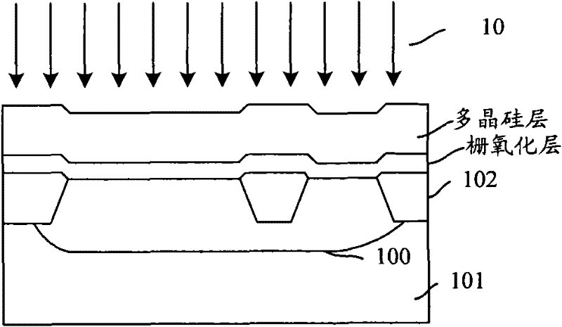
[0031] However, the VT junction depth of the semiconductor device obtained by this method is relatively deep. This is because, during the VT ion implantation process, the dopants are concentrated in the region close to the semiconductor substrate 101, so that the VT junction depth is shallow. , but in the subsequent rapid thermal annealing, such as the rapid thermal annealing in step 6 or step 8, since the semiconductor substrate is combined with ordered polysilicon, the high-concentration dopant in the deep region of the VT junction will diffuse to the surroundings, increasing the The depth of the VT junction is increased, which causes a reverse current between the source and the drain, increasing the leakage current
[0032] At present, this problem can be solved by reducing the dose and energy of VT ion implantation. However, since the final concentration of the VT ion implantation dopant formed on the semiconductor substrate is used to prevent gate penetration and prevent the occurrence of leakage current, Reducing the dose and energy of VT ion implantation will reduce the concentration of the final VT junction, which will cause the risk of gate penetration and increase the leakage current

Method used


Image

  • Method for improving junction depth property of semiconductor device
  • Method for improving junction depth property of semiconductor device
  • Method for improving junction depth property of semiconductor device

Examples


Embodiment Construction

[0053] In order to make the object, technical solution and advantages of the present invention clearer, the present invention will be further described in detail below with reference to the accompanying drawings and examples.

[0054] It can be seen from the prior art that the reason why the VT junction depth of the semiconductor device is relatively deep is mainly because: after the VT ion implantation is completed, when the subsequent rapid thermal annealing is performed, as in step 6 or step 8 of the prior art Rapid thermal annealing, because the semiconductor substrate is combined with ordered polysilicon, will make the high-concentration dopants in the deep region of the VT junction diffuse to the surroundings, increasing the depth of the VT junction, thereby causing a reverse current between the source and the drain , increasing the leakage current.

[0055] Therefore, in order not to reduce the concentration of the VT junction, the present invention makes the depth of t...


PUM


Abstract

The invention discloses a method for improving junction depth property of a semiconductor device. The method comprises the following steps of: after ion implantation of semiconductor dopants is performed on a substrate of the semiconductor device, forming a well on the substrate of the semiconductor device; forming an isolated shallow groove on the substrate of the semiconductor device, and then forming a grid on the substrate of the semiconductor device; re-oxidizing the surface of the grid and the surface of the substrate of the semiconductor device, and then lightly doping the grid and thesubstrate of the semiconductor device; forming a nitrogen oxide side wall of the grid, doping the grid and the substrate of the semiconductor device, forming a drain and a source by deposition on thesemiconductor device, and performing quick thermal annealing; and depositing metals on the surface of the grid and the semiconductor substrate by adopting a self-alignment silicide method to form metal silicon layers, then performing quick annealing treatment, and etching the un-reacted metals. By the method provided by the invention, the junction depth of the semiconductor device becomes light, and the device performance of the manufactured semiconductor device is improved.

Description

technical field [0001] The invention relates to semiconductor manufacturing technology, in particular to a method for improving junction depth characteristics of semiconductor devices. Background technique [0002] With the wide application of electronic equipment, the manufacturing process of semiconductors has been developed rapidly, the feature size of semiconductor devices is getting smaller and smaller, and the manufacturing of device layers in semiconductor devices is becoming more and more important. The device layer of the semiconductor device here refers to the manufacturing of the source, drain and gate on the semiconductor substrate. Among them, the threshold voltage (VT) node depth characteristic of the device layer of the semiconductor device becomes a key factor affecting the performance of the device layer of the final semiconductor device. The deep VT junction region is between the source and drain of the semiconductor device, close to the surface of the sem...

Claims


Application Information

Patent Timeline
Patent Type & Authority Patents(China)
IPC IPC(8): H01L21/336H01L21/265
Inventor 赵猛张立夫
Owner SEMICON MFG INT (SHANGHAI) CORP
Learn More