Manufacturing method of novel gallium nitride LED (light emitting diode) chip electrode structure

A technology of LED chip and electrode structure, applied in circuits, electrical components, semiconductor devices, etc., can solve problems such as difficulty in heat dissipation, and achieve the effects of solving uneven heat dissipation, increasing heat dissipation area, and improving heat dissipation efficiency

Inactive Publication Date: 2011-05-18
JIANGXI LIANCHUANG OPTOELECTRONIC SCIENCE AND TECHNOLOGY CO LTD
View PDF3 Cites 5 Cited by
  • Summary
  • Abstract
  • Description
  • Claims
  • Application Information

AI Technical Summary

Problems solved by technology

[0003] The purpose of the present invention is to provide a method for manufacturing a novel GaN-based LED chip electrode structure, through the improvement of the LED chip electrode structure, greatly improve the heat dissipation efficiency of the LED chip, and effectively solve the problems existing in the traditional GaN-based blue LED chip structure. Difficult heat dissipation, so that it can be applied to the production of high-power GaN-based LED chips under high-current working conditions

Method used


Image

  • Manufacturing method of novel gallium nitride LED (light emitting diode) chip electrode structure
  • Manufacturing method of novel gallium nitride LED (light emitting diode) chip electrode structure

Examples


Embodiment Construction

[0016] The specific embodiment of the present invention is as shown in the accompanying drawings.

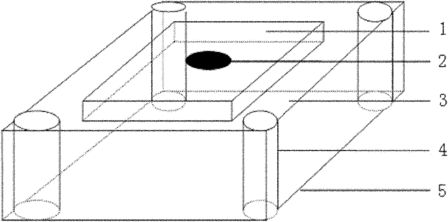
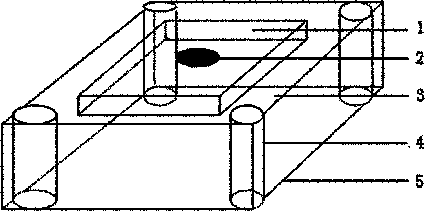
[0017] First, take an epitaxial wafer with GaN epitaxial layer grown on the sapphire substrate by MOCVD method, and selectively etch and remove the P-type layer in the epitaxial layer by dry etching according to the designed chip electrode structure 1. Exposing the N-type epitaxial layer 3; then forming an ohmic contact between the ITO diffusion layer and the P-type layer on the surface of the P-type epitaxial layer 1 of the epitaxial wafer, and using laser drilling technology at the four corners of the exposed N-type epitaxial layer 3 chip Drill holes perpendicular to the surface of the epitaxial wafer, the depth of the hole is 120um, and the diameter of the hole is 50um; the thickness of the epitaxial wafer after the above operations is reduced to about 120um, so that the hole punched in the previous step becomes a through hole connecting the surface of the substrate and the N-...


PUM


Abstract

The invention relates to a manufacture method of a novel gallium nitride LED (light emitting diode) chip electrode structure. The method comprises the following steps: taking a gallium nitride epitaxial wafer with a sapphire substrate, selectively etching according to the chip architecture to remove a P type layer 1 in the epitaxial layer and expose an N type epitaxial layer 3; forming an ITO (indium tin oxide) diffusion layer in ohmic contact with the P type layer, on the surface of the P type epitaxial layer 1 of the epitaxial wafer, punching a hole in the exposed N type epitaxial layer region; thinning the epitaxial wafer, so that the punched hole becomes a through hole 4 communicating the substrate surface with an N type region; coating a Cr layer on the surface of the epitaxial layer by vaporization through an vacuum coating technology firstly, then coating an Au layer by vaporization, forming a required weld line electrode 2 of the LED by photoetching and etching technologies; depositing an AL metal layer 5 on the surface of the thinned substrate, and forming a reflector of the LED chip; and splitting the epitaxial wafer to form LED chips which can be directly packaged and applied. The manufacture method in the invention is suitable for preparing high-power LED chips of a gallium nitride luminescent material.

Description

technical field [0001] The invention relates to a method for manufacturing an electrode structure of a GaN-based LED chip, belonging to the field of semiconductor LED chip manufacturing. Background technique [0002] The development of light-emitting diodes (LEDs) based on gallium nitride (GaN) materials is a major achievement in the progress of optoelectronic science and technology. GaN series LEDs are key light sources for the development of solid-state lighting and the realization of the human lighting revolution, and have broad application prospects. Conventional LEDs have low luminous power and cannot meet the requirements of LED lighting applications. To increase the luminous power, it is necessary to increase the brightness by increasing the current without changing the material. However, as the current flowing into the LED chip increases, the heat generated by the LED will increase sharply, resulting in changes and attenuation of the performance of the LED device. T...

Claims


Application Information

Patent Timeline
Patent Type & Authority Applications(China)
IPC IPC(8): H01L33/00H01L33/36
Inventor 万金平任强万义朋何民华
Owner JIANGXI LIANCHUANG OPTOELECTRONIC SCIENCE AND TECHNOLOGY CO LTD
Why Eureka
Try Eureka