Trench metal-oxide semiconductor field effect transistor (MOSFET) and manufacture method thereof

A technology of oxide semiconductors and field effect transistors, which is applied in semiconductor/solid-state device manufacturing, semiconductor devices, semiconductor/solid-state device components, etc., and can solve problems such as low yield and reliability

Inactive Publication Date: 2011-06-15
FORCE MOS TECH CO LTD
View PDF1 Cites 19 Cited by
  • Summary
  • Abstract
  • Description
  • Claims
  • Application Information

AI Technical Summary

Problems solved by technology

[0004] figure 2 The disadvantage of the N-channel trench MOSFET shown in the prior art is that the contact area uses a planar contact instead of the good performance trench contact
If trench contacts are used in this structure, such as image 3 As shown, as far as the ESD protection diode is concerned, the additional silicon etch will easily penetrate the gate oxide layer 130' and extend into the P-type body region 116 under the ESD protection diode, causing a short circuit between the gate and the source. connection, resulting in low yield and reliability

Method used


Image

  • Trench metal-oxide semiconductor field effect transistor (MOSFET) and manufacture method thereof
  • Trench metal-oxide semiconductor field effect transistor (MOSFET) and manufacture method thereof
  • Trench metal-oxide semiconductor field effect transistor (MOSFET) and manufacture method thereof

Examples


Embodiment Construction

[0055] The invention will be described in detail below with reference to the accompanying drawings, in which preferred embodiments of the invention are shown. The invention can, however, be embodied in different ways and should not be limited to the embodiments described herein. For example, the description here refers more to N-channel trench MOSFETs, but clearly other devices are possible.

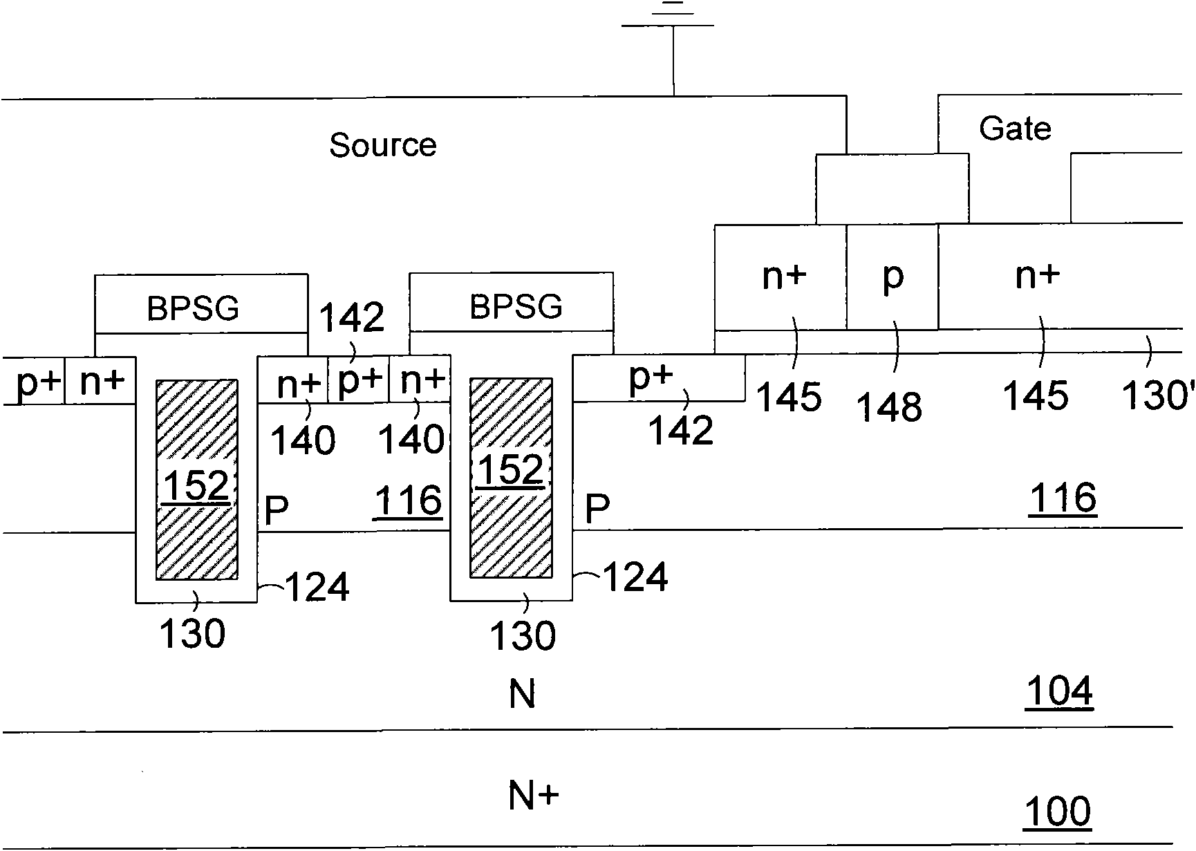
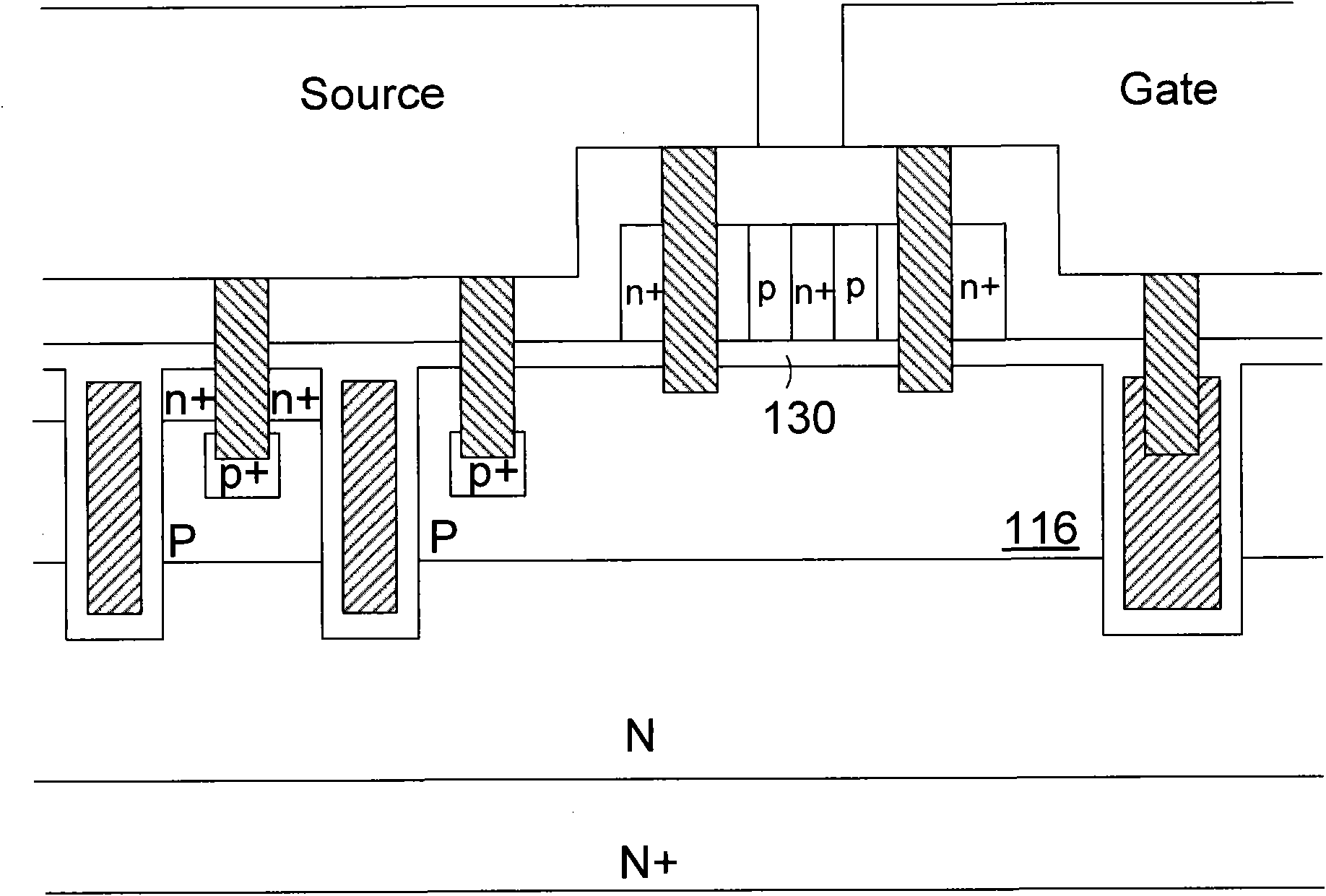
[0056] refer to Figure 4 In a preferred embodiment of the present invention shown, an N-type epitaxial layer 204 is formed on an N+ substrate 200, and in the N-type epitaxial layer 204, there are a plurality of first trench gates 210 located in the active region , at least one wider second trench gate 212 for gate connection and at least two third trench gates 211 located below the ESD contact trench. The inner surfaces of the first trench gate 210 , the second trench gate 212 and the third trench gate 211 are lined with a gate oxide layer 230 and filled with doped polysilicon. Meanw...


PUM


Abstract

The invention discloses a trench metal-oxide semiconductor field effect transistor (MOSFET) and a manufacture method thereof. The trench MOSFET comprises ESD (Electro-Static Discharge) protection diodes, and a trench grid arranged below each ESD contact trench is used as a buffer layer to avoid the short circuit between a source electrode and a grid electrode.

Description

technical field [0001] The invention relates to a unit structure, device structure and process manufacturing of a semiconductor power device, in particular to a unit structure and a process method of a trench MOSFET (Metal Oxide Semiconductor Field Effect Transistor). Background technique [0002] The design and manufacturing technology of traditional semiconductor power devices is subjected to increasingly severe tests in terms of ESD (Electrostatic Discharge, electrostatic discharge) protection. Especially, in the trench MOSFET, the high-voltage transient signal generated by electrostatic discharge will generate a strong voltage of more than 10,000 volts on the gate insulating layer, and cause unpredictable damage to the trench MOSFET. damage. In order to reduce the impact caused by electrostatic discharge, many trench MOSFETs in the prior art are designed as systems with their own ESD protection, where a typical ESD protection structure consists of multiple back-to-back ...

Claims


Application Information

Patent Timeline
Patent Type & Authority Applications(China)
IPC IPC(8): H01L27/06H01L23/528H01L21/82H01L21/768
CPCH01L2924/0002
Inventor 谢福渊
Owner FORCE MOS TECH CO LTD
Why Eureka
Try Eureka