Light-emitting diode chip bonding method, bonded light-emitting diode and chip structure

A light-emitting diode and chip structure technology, which is applied in the field of light-emitting diode chip solidification, solid-state light-emitting diode and chip structure, can solve the problems of shortened service life, poor heat resistance and thermal conductivity of polymer conductive adhesive, chip structure and substrate Reduced contact reliability and other problems, to achieve the effect of shortening the pre-fixing time and good reliability

Active Publication Date: 2011-06-22
IND TECH RES INST
View PDF17 Cites 10 Cited by
  • Summary
  • Abstract
  • Description
  • Claims
  • Application Information

AI Technical Summary

Problems solved by technology

[0010] In view of the above problems, the technical problem to be solved by the present invention is to provide a chip structure, so as to improve the existing chip structure. The problem of reduced performance and shortened service life; and the use of metal soldering materials, resulting in the residual thermal stress of the chip structure during the die-bonding process and the problem of reduced reliability of the joint between the chip structure and the substrate after the die-bonding

Method used


Image

  • Light-emitting diode chip bonding method, bonded light-emitting diode and chip structure
  • Light-emitting diode chip bonding method, bonded light-emitting diode and chip structure
  • Light-emitting diode chip bonding method, bonded light-emitting diode and chip structure

Examples


Embodiment Construction

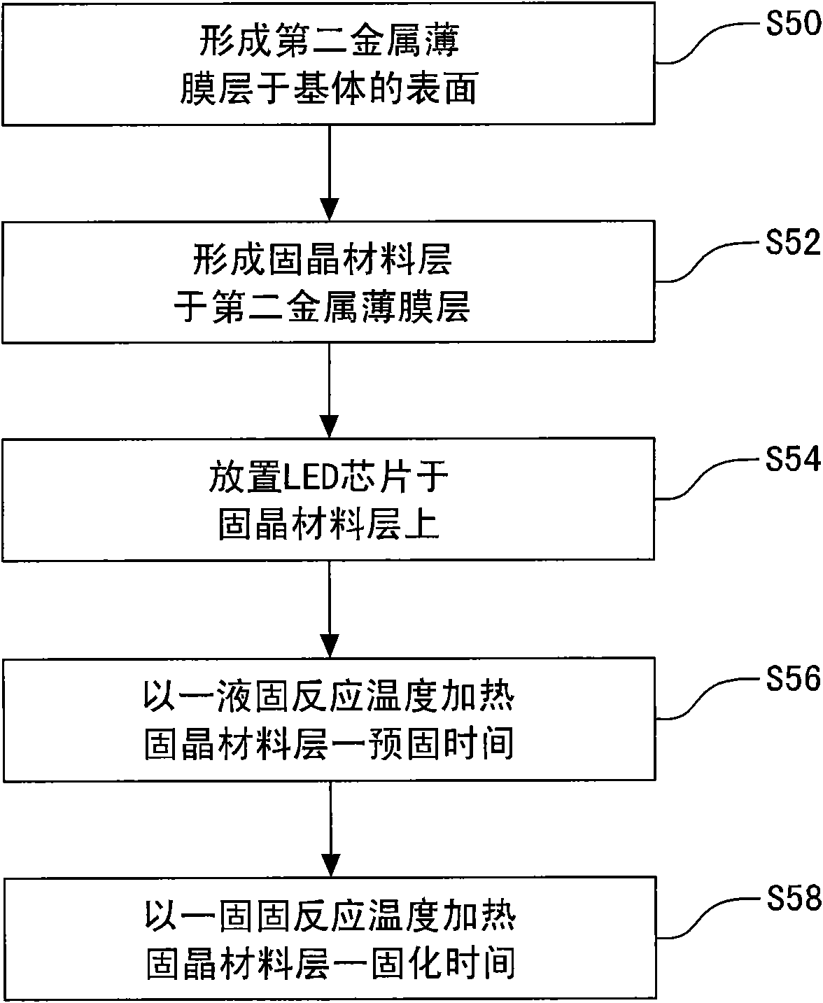
[0060] Below in conjunction with accompanying drawing, structural principle and working principle of the present invention are specifically described:

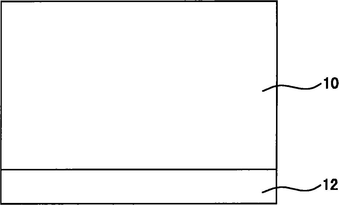
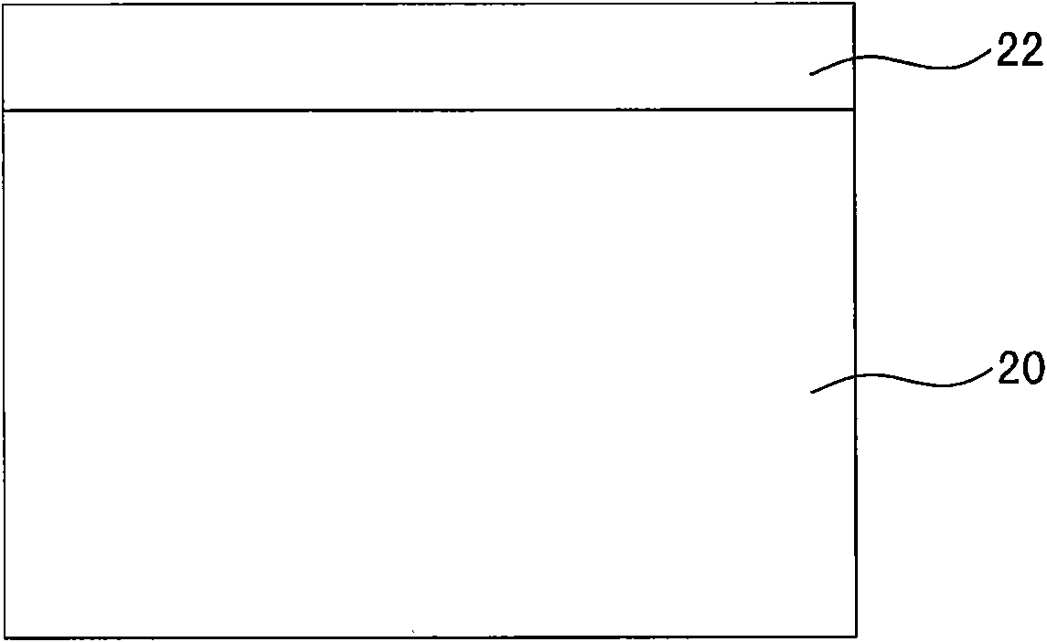
[0061] First, see figure 1 , Figure 2A and Figure 2B . figure 1 It is a schematic flowchart of an embodiment of a method for bonding a light-emitting diode (LED) chip according to the present invention. Figure 2A It is a schematic structural diagram of an LED chip according to an embodiment of the crystal bonding method of the present invention. Figure 2B It is a schematic structural diagram of a substrate according to an embodiment of the crystal bonding method of the present invention.

[0062] This LED chip bonding method is suitable for combining the LED chip 10 and the substrate 20 . The LED chip 10 can be an LED with a p-i-n structure, such as but not limited to gallium nitride (GaN), gallium indium nitride (GaInN), aluminum indium gallium phosphide (AlInGaP) and aluminum indium gallium nitride (AlInGaN), nitrid...


PUM


Abstract

The invention discloses a light-emitting diode chip bonding method, a bonded light-emitting diode and a chip structure. The light-emitting diode chip bonding method is suitable for bonding a light-emitting diode chip on a substrate. The light-emitting diode chip is provided with a first metal film layer. The chip structure comprises a chip and a bonding material layer, wherein the bonding material layer is arranged on one side of the chip. The bonding method comprises the following steps of: forming a second metal film layer on the surface of the substrate; forming the bonding material layer on the second metal film layer; placing the light-emitting diode chip on the bonding material layer and making the first metal film layer contact the bonding material layer; heating the bonding material layer for a pre-curing time at a liquid-solid reaction temperature to form a first intermetallic layer and a second intermetallic layer; and heating the bonding material layer for a curing time at a solid-solid reaction temperature to perform a solid-solid reaction. The liquid-solid reaction temperature and the solid-solid reaction temperature are both lower than 110 DEG C; and the melting points of the first intermetallic layer and the second intermetallic layer after the solid-solid reaction are higher than 200 DEG C.

Description

technical field [0001] The present invention relates to a bonding method (bonding method) of a light emitting diode chip (chip), a light emitting diode and a chip structure, in particular to a bonding method capable of low-temperature bonding and obtaining a high-temperature intermetallic layer, and a bonding method with the bonding method. structure of light-emitting diodes and chip structures. Background technique [0002] The technology of attaching light emitting diode (LED, Light Emitting Diode) chips to the lead frame has been developed for many years, and can be roughly divided into two types according to the different bonding materials. The first type is polymer conductive adhesive material, and the second type is metal welding material. [0003] The aforementioned first category can be found in Taiwan Patent No. 463394 "Chip-Type Light-Emitting Diode and Its Manufacturing Method". It is mainly to plate silver on the surface of a metal substrate, and form a plurali...

Claims


Application Information

Patent Timeline
Patent Type & Authority Applications(China)
IPC IPC(8): H01L33/00H01L33/62
CPCH01L24/83H01L24/29H01L2224/8381H01L2224/83825H01L2924/14H01L2924/00
Inventor 林修任林建宪郑佳申陈効义
Owner IND TECH RES INST
Why Eureka
Try Eureka