Method for preparing chalcopyrite solar cell light absorption layer and cell thereof

A technology for solar cells and light absorbing layers, which is applied in the manufacturing of circuits, electrical components, and final products, etc., can solve the problems of insufficient uniformity of the light absorbing layer, and achieve the effects of single crystal phase, good crystallinity, and improved uniformity.

Inactive Publication Date: 2011-07-06
BYD CO LTD
View PDF0 Cites 5 Cited by
  • Summary
  • Abstract
  • Description
  • Claims
  • Application Information

AI Technical Summary

Problems solved by technology

[0007] In order to solve the technical problem that the uniformity of the light-absorbing layer prepared in the prior art is not good enough, the present invention provides a method for preparing a chalcopyrite-type solar cell light-absorbing layer with further improved uniformity

Method used


Image

  • Method for preparing chalcopyrite solar cell light absorption layer and cell thereof
  • Method for preparing chalcopyrite solar cell light absorption layer and cell thereof
  • Method for preparing chalcopyrite solar cell light absorption layer and cell thereof

Examples


preparation example Construction

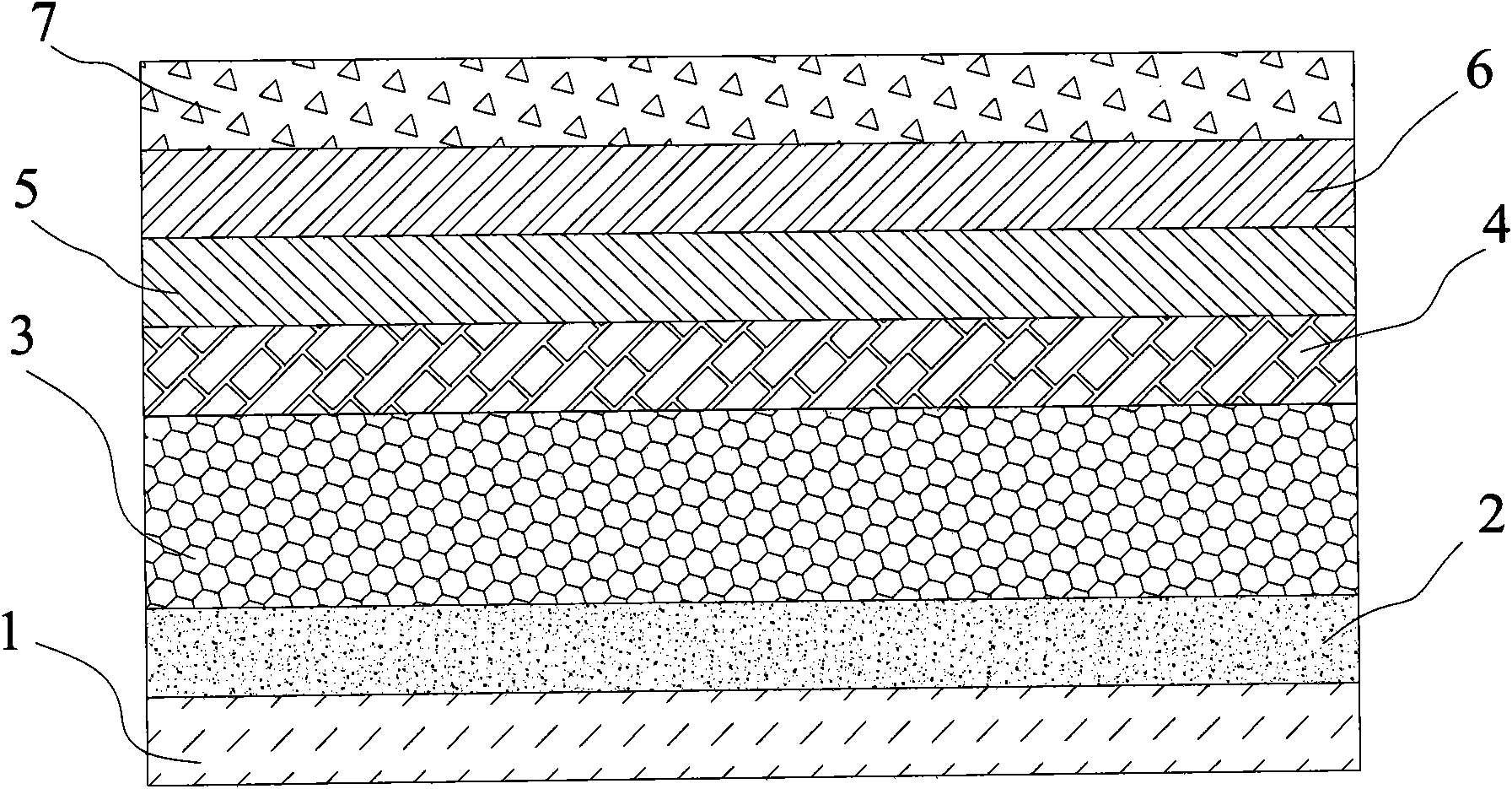
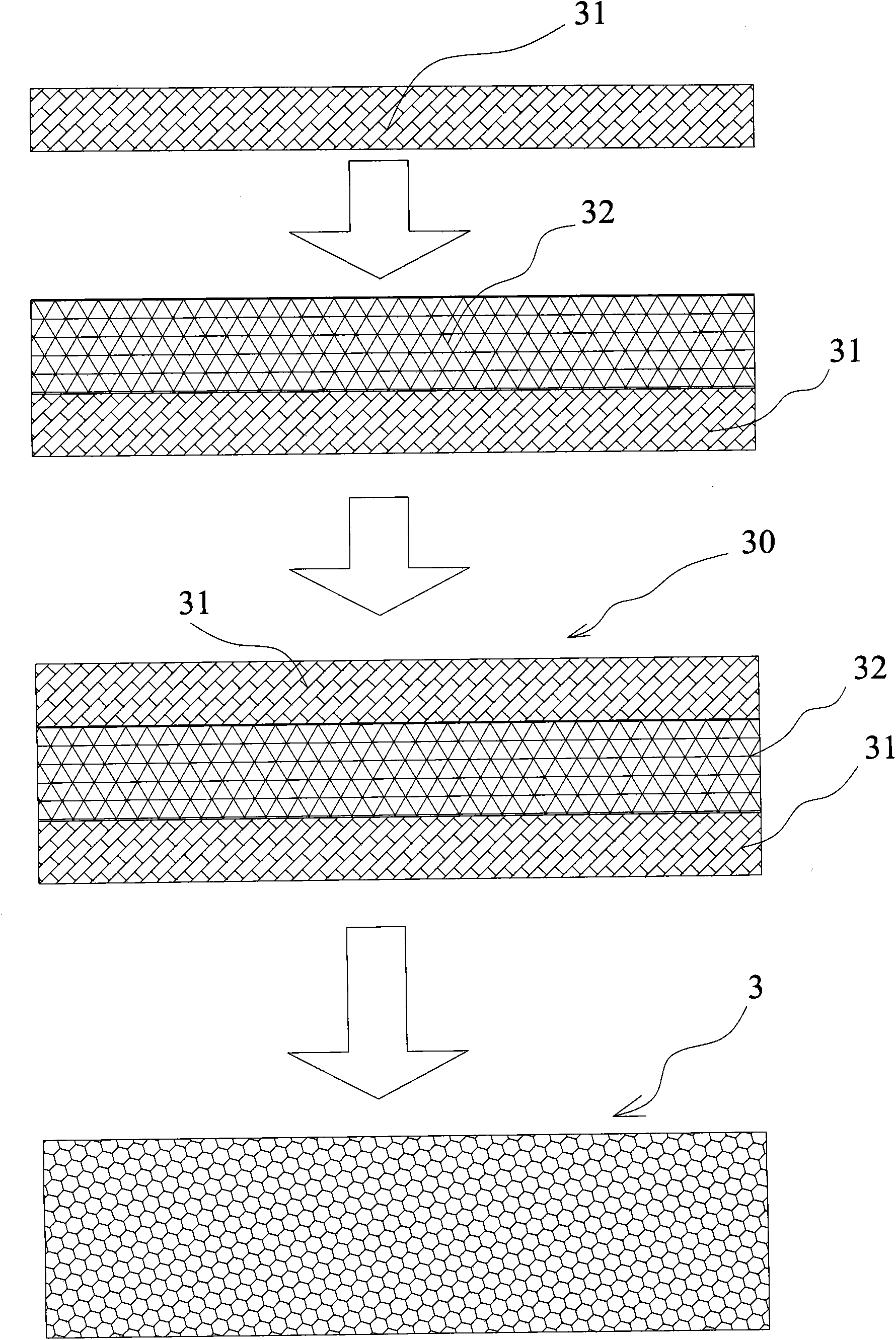
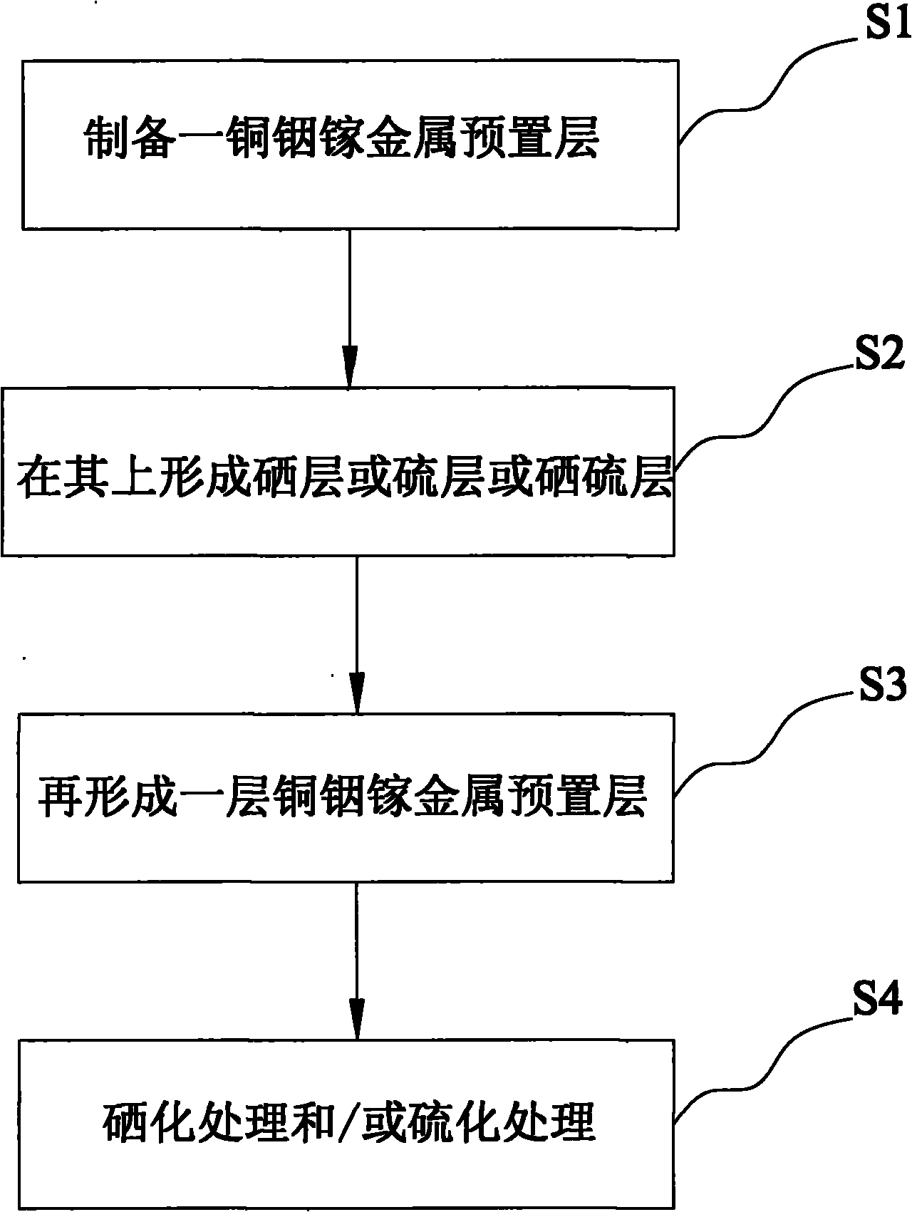
[0036] The preparation method of the light absorption layer of chalcopyrite-type solar cell, the preparation process is as follows image 3 As shown, you can visually refer to the diagram of its preparation method, such as figure 2 As shown, including the following steps:

[0037] S1: Preparation of a metal pre-layer 31; its material is copper indium or copper indium gallium, copper indium gallium is actually only part of gallium replaced part of indium, and its production method is generally to pass directly on the substrate deposited with the metal back electrode The magnetron sputtering method deposits a layer of copper indium or copper indium gallium. This metal pre-layer is also called a precursor film in the art.

[0038] When the material of the metal pre-layer 31 is copper indium, the copper indium metal pre-layer 31 is generally prepared by sputtering a copper indium target material to deposit a copper indium film. The selenized chalcopyrite-type solar cell is called cop...

Embodiment 1

[0051] The method for preparing a copper indium gallium selenium solar cell in this example: sputtering and depositing a 1.0 μm Mo back electrode layer on the soda lime glass, and then depositing a 0.5 μm CuInGa metal layer on the Mo layer with DC magnetron sputtering, and then RF magnetron sputtering Depositing a 0.5μm Se layer and finally sputtering a 0.5μm CuInGa layer, and then baking the substrate by an iodine tungsten lamp or other light source. The heating trend is: heating from room temperature for 5 minutes to 350°C and holding at this temperature for 3 to 5 minutes, Then the temperature was raised to 500°C and kept at a constant temperature for 20 minutes to form a light absorption layer, and then the film was stepped down to 350°C within 20 minutes and then naturally cooled to room temperature. The constant temperature process is carried out in a selenium atmosphere.

[0052] The crystal structure of the thin film was tested by XRD and the results are as follows Figur...

Embodiment 2

[0054] The method of preparing a copper indium gallium sulfur solar cell in this example: sputtering and depositing a 1.0 μm Mo back electrode layer on the soda lime glass, and then depositing a CuInGa metal layer 0.4 μm on the Mo layer by DC magnetron sputtering, and then RF magnetron sputtering Depositing the 0.8μm S layer and finally sputtering the 0.6μm CuInGa layer, and then baking the substrate by an iodine tungsten lamp or other light source. The heating trend is: heating from room temperature for 5 minutes to 350°C and holding it at this temperature for 3 to 5 minutes. Then the temperature was raised rapidly to 550°C and kept at a constant temperature for 20 minutes to form a CIGS absorption layer, and then the film was stepped down to 350°C in 20 minutes and then naturally cooled to room temperature. The 550°C constant temperature process is all completed in a sulfur atmosphere.

[0055] The crystal structure of the thin film was tested by XRD and the results are as foll...


PUM


Abstract

The invention provides a method for preparing a chalcopyrite solar cell light absorption layer with further enhanced uniformity and a solar cell thereof to solve a technical problem in the prior art that the prepared light absorption layer has not good enough uniformity. The method for preparing chalcopyrite solar cell light absorption layer comprises the following steps of: S1, preparing a metal preset layer; S2, forming a selenium layer or a sulfur layer or a selenium sulfur layer on the surface of the metal preset layer; S3, forming a metal preset layer on the selenium layer or the sulfur layer or the selenium sulfur layer in the step S2 to form an A/B/A sandwich -shaped intermediate product; and S4, carrying out selenylation and/or sulfurization treatment on the intermediate product. By utilizing the A/B/A sandwich-shaped structure, a layer of Se or S or a SeS layer is arranged between two metal preset layers; therefore, the internal reaction can be more sufficient in the selenylation and/or sulfurization process; the uniformity is further enhanced; the crystallization is better; and a single crystalline phase is achieved.

Description

Technical field [0001] The invention belongs to the field of solar cells, in particular to the field of thin-film solar cells, especially the field of thin-film solar cells with a chalcopyrite-type light absorption layer. Background technique [0002] In modern society, energy is increasingly valued by people. With the gradual consumption of non-renewable resources such as oil and coal, people think that renewable resources are the main energy sources for us in the future, such as wind energy, water energy, and solar energy. The existing way of using solar energy is generally to absorb light energy through semiconductor materials and then store it in a battery, which is called a solar cell. Solar cells currently include silicon solar cells, thin-film solar cells and so on. [0003] Crystalline silicon solar cells are now widely used, and thin-film solar cells are increasingly familiar to people. The common compound semiconductor copper indium selenide CuInSe with chalcopyrite stru...

Claims


Application Information

Patent Timeline
Patent Type & Authority Applications(China)
IPC IPC(8): H01L31/18
CPCY02P70/50
Inventor 刘国文钟北军马青云
Owner BYD CO LTD
Why Eureka
Try Eureka