Low-voltage organic thin-film transistor and preparation method thereof

An organic thin film and transistor technology, applied in the field of low-voltage organic thin film transistors and their preparation, can solve the problem of high working voltage, and achieve the effects of lowering voltage, lower surface roughness, and increasing capacitance

Inactive Publication Date: 2011-07-06
INST OF MICROELECTRONICS CHINESE ACAD OF SCI
View PDF2 Cites 15 Cited by
  • Summary
  • Abstract
  • Description
  • Claims
  • Application Information

AI Technical Summary

Problems solved by technology

[0005] In view of this, the main purpose of the present invention is to provide a low-voltage organic thin film transistor, to solve the pro

Method used


Image

  • Low-voltage organic thin-film transistor and preparation method thereof
  • Low-voltage organic thin-film transistor and preparation method thereof
  • Low-voltage organic thin-film transistor and preparation method thereof

Examples


Embodiment Construction

[0039] The technical solution of the present invention will be further described in detail below in conjunction with the accompanying drawings and the embodiments of the present invention.

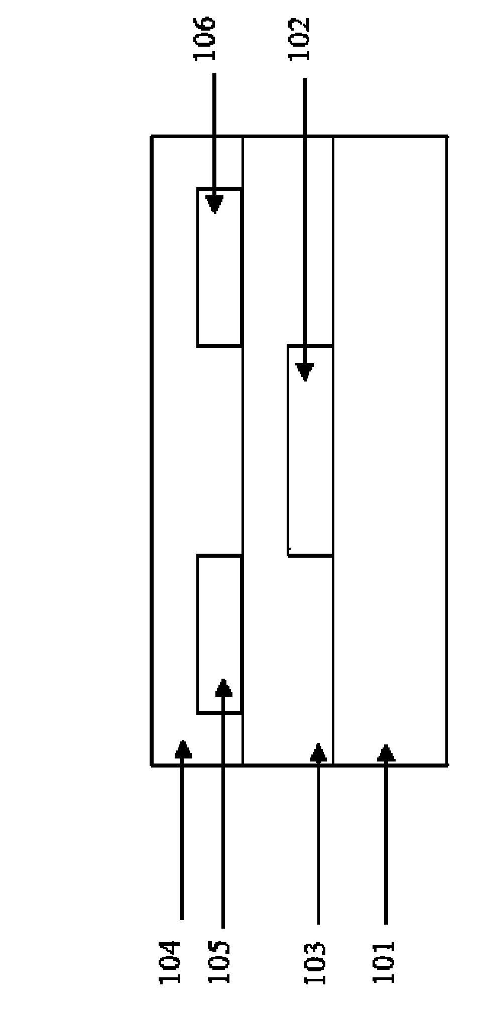
[0040] The structure of the low-voltage organic thin film transistor provided by Embodiment 1 of the present invention is as follows: figure 1 As shown, wherein the insulating substrate 101 is located at the bottom of the organic thin film transistor device, the gate electrode 102 is located on the insulating substrate 101, the gate dielectric 103 covers the insulating substrate 101 and the gate electrode 102, and an active layer is prepared on the surface of the gate dielectric 103. The electrode 105 and the drain electrode 106 ; the source electrode 105 and the drain electrode 106 respectively cover the top surface of the gate dielectric 103 ; the organic semiconductor layer 104 covers the gate dielectric 103 , the source electrode 105 and the drain electrode 106 .

[0041] For the low-v...


PUM

PropertyMeasurementUnit
Thicknessaaaaaaaaaa

Abstract

The invention discloses a low-voltage organic thin-film transistor and a preparation method thereof, belonging to the technical field of organic electronics. The organic thin-film transistor comprises an insulating substrate, a gate electrode on the insulating substrate, gate dielectrics covering the insulating substrate and the gate electrode, a source electrode and a leakage electrode on the gate dielectric and organic semiconductor layers covering the gate dielectric, the source electrode and the leakage electrode. The preparation method comprises the steps of: firstly, preparing the gate electrode on the insulating substrate; secondly, preparing dielectric layers on the surfaces of the insulating substrate and the gate electrode; then, preparing the source electrode and the leakage electrode on the dielectric layers; and finally, depositing the organic semiconductor layers on the dielectric layer, the source electrode and the leakage electrode to complete the preparation of the device. In the invention, by utilizing an atomic layer deposition method, thinner metallic oxide films are prepared to serve as the dielectric layers and the capacitance of the organic thin-film transistor device is greatly increased, therefore, the voltage of the device is reduced and the organic thin-film transistor with low working voltage can be obtained.

Description

technical field [0001] The invention belongs to the technical field of organic electronics, and in particular relates to a low-voltage organic thin film transistor and a preparation method thereof. Background technique [0002] With the deepening of information technology, electronic products have entered all aspects of people's work and life. In daily life, people have more and more demands for low-cost, flexible, low-weight, and portable electronic products. Traditional devices and circuits based on inorganic semiconductor materials are difficult to meet the above requirements of electronic products. However, the use of organic polymer-based Organic microelectronics technology based on semiconductor materials can meet the requirements of low cost, flexibility, and portability of electronic products. Therefore, organic microelectronics technology has received more and more attention under the development trend of this technology. [0003] Organic thin film transistors are ...

Claims


Application Information

Patent Timeline
IPC IPC(8): H01L51/05H01L51/30H01L51/40
Inventor 商立伟姬濯宇刘明
Owner INST OF MICROELECTRONICS CHINESE ACAD OF SCI
Why Eureka
Try Eureka