Rear through-hole interconnected wafer level MOSFET (metal oxide semiconductor field effect transistor) packaging structure and implementation method

A technology of packaging structure and implementation method, applied in electrical components, electrical solid devices, circuits, etc., can solve the problems of restricting the performance improvement of MSOFET, unable to conduct or dissipate heat from the chip, and increase the size of the device, so as to shorten the interconnection distance, Improve the current carrying capacity and enhance the effect of conduction

Active Publication Date: 2012-09-19
JIANGYIN CHANGDIAN ADVANCED PACKAGING CO LTD
View PDF0 Cites 0 Cited by
  • Summary
  • Abstract
  • Description
  • Claims
  • Application Information

AI Technical Summary

Problems solved by technology

However, traditional MOSFET packages are mainly in the form of TO, SOT, SOP, QFN, QFP, etc. This type of package wraps the chip in a plastic package, which cannot conduct or dissipate the heat generated by the chip in time, which restricts the performance improvement of the MSOFET.
Moreover, the plastic packaging itself increases the size of the device, which does not meet the requirements of the development of semiconductors in the direction of light, thin, short, and small
As far as the packaging process is concerned, this type of packaging is based on a single chip, which has the problems of low production efficiency and high packaging cost

Method used


Image

  • Rear through-hole interconnected wafer level MOSFET (metal oxide semiconductor field effect transistor) packaging structure and implementation method
  • Rear through-hole interconnected wafer level MOSFET (metal oxide semiconductor field effect transistor) packaging structure and implementation method
  • Rear through-hole interconnected wafer level MOSFET (metal oxide semiconductor field effect transistor) packaging structure and implementation method

Examples


Embodiment Construction

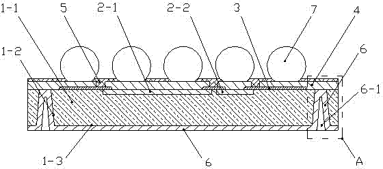
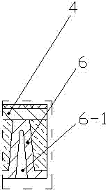
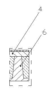
[0024] see figure 1 , figure 1 It is a cross-section schematic diagram of the through-hole interconnection type wafer-level MOSFET packaging structure of the present invention. Depend on figure 1 It can be seen that the packaging structure of the wafer-level MOSFET with post-via interconnection in the present invention includes a chip body 1-1, a chip through hole 1-2, a chip source electrode 2-1, a chip gate electrode 2-2, and a chip surface protection layer. 3. Front circuit layer 4 , circuit surface protection layer 5 , solder balls 7 and circuit layer 6 . The chip source electrode 2-1 and the chip gate electrode 2-2 are arranged on the front of the chip body 1-1, and the chip surface protective layer 3 is arranged on the front of the chip body 1-1, the chip source electrode 2-1 and the chip gate electrode 2-2; The front circuit layer 4 is arranged on the surface of the chip body 1-1, the chip source electrode 2-1, the chip gate electrode 2-2 and the chip surface protect...


PUM


Abstract

The invention relates to a rear through-hole interconnected wafer level MOSFET (metal oxide semiconductor field effect transistor) packaging structure and an implementation method. A chip source electrode (2-1) and a chip gate electrode (2-2) are arranged on the front surface of a chip body (1-1); chip surface protecting layers (3) are arranged on the front surfaces of the chip body, the chip source electrode and the chip gate electrode; front surface circuit layers (4) are arranged on the surfaces of the chip body, the chip source electrode, the chip gate electrode and the chip surface protecting layers; circuit surface protecting layers (5) are arranged on the surfaces of the front surface circuit layers and the chip surface protecting layers; solder balls (7) are arranged on the surfaces of the front surface circuit layers; a chip through hole (1-2) is arranged by penetrating the front surface and the back surface of the chip body; and a circuit layer (6) is arranged on the back surface of the chip body, the circuit layer (6) is filled in the chip through hole, and the circuit layer filled in the chip through hole is in direct contact with the side wall of the chip through holeand interconnected with the front surface circuit layers. According to the invention, the packaging structure has high performance; and the process method which is used for implementing the structureand has the advantages of high production efficiency and low packaging cost.

Description

technical field [0001] The invention relates to a wafer level chip size packaging structure and a realization method. It belongs to the technical field of semiconductor packaging. Background technique [0002] MOSFET (Metal Oxide Semiconductor Field Effect Transistor) is a field effect transistor that uses electric field effects to control semiconductors. MOSFETs have received increasing attention in recent years due to their characteristic of enabling low power consumption voltage control. The performance of MOSFET, especially the current carrying capacity, largely depends on the heat dissipation performance, and the heat dissipation performance mainly depends on the package form. However, traditional MOSFET packages are mainly in the form of TO, SOT, SOP, QFN, QFP, etc. This type of package wraps the chip in a plastic package, which cannot conduct or dissipate the heat generated by the chip in time, which restricts the performance improvement of the MSOFET. . Moreover,...

Claims


Application Information

Patent Timeline
Patent Type & Authority Patents(China)
IPC IPC(8): H01L29/78H01L23/367H01L29/417H01L23/482H01L21/50H01L21/60
CPCH01L2224/13H01L2924/13091
Inventor 陈栋胡正勋张黎陈锦辉赖志明
Owner JIANGYIN CHANGDIAN ADVANCED PACKAGING CO LTD
Why Eureka
Try Eureka