Current regulation diode chip and manufacturing method thereof

A technology of current regulation and diodes, which is applied in semiconductor/solid-state device manufacturing, circuits, electrical components, etc. It can solve the problems of small anode area, short circuit, and inability to achieve low-cost packaging, and achieve the effect of convenient packaging

Active Publication Date: 2011-07-20
ZHEJIANG MINGDE MICROELECTRONICS CO LTD
View PDF4 Cites 10 Cited by
  • Summary
  • Abstract
  • Description
  • Claims
  • Application Information

AI Technical Summary

Problems solved by technology

[0004] However, due to the small area of ​​the anode, such a structure cannot realize double-sided brazing interconnection of low-cost packaging (such as the plastic packaging of general rectifier chips), and it only needs to be tightened by two leads with plugs to complete the interconnection without welding. Glass encapsulation (such as low-power voltage adjustment diodes)
The reason is that the metal layer 10 of the drain region and the interconnection metal layer 9b of the source, gate, and substrate will be short-circuited during such packaging.

Method used


Image

  • Current regulation diode chip and manufacturing method thereof
  • Current regulation diode chip and manufacturing method thereof
  • Current regulation diode chip and manufacturing method thereof

Examples


Embodiment Construction

[0023] The following is attached figure 2 to attach Figure 9 Embodiments of the present invention are further described in detail.

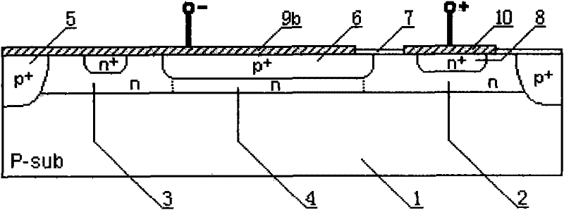
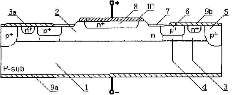
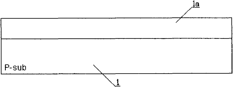
[0024] The present invention is a current regulating diode chip, which includes a substrate layer 1 and an epitaxial layer 1a covering it, and selects an applicable special-shaped epitaxial wafer according to the parameter requirements of the CRD and the height of the mesa. In this embodiment, the epitaxial layer 1a It is N-type, and the substrate layer 1 is highly doped P-type.

[0025] A drain region 2 is formed on the epitaxial layer 1a, and the surface of the drain region 2 is further provided with a first ohmic contact diffusion layer 8 and a first metal layer 10 covering the first ohmic contact diffusion layer 8 .

[0026] The drain region 2 is in the shape of a mesa, and its height is greater than 2 microns. The mesa shape is etched on the epitaxial layer by the method of silicon homogeneous etching or anisotropic etching. The function...


PUM


Abstract

The invention discloses a current regulation diode chip, which comprises a substrate layer and an epitaxial layer covered on the substrate layer, wherein a drain region is formed on a central area of the epitaxial layer, and a first ohmic contact diffusion layer and a first metal layer covered on the first ohmic contact diffusion layer are arranged on the surface of the drain region further; an annular P-type grid region and a channel positioned below the P-type grid region are respectively formed on the outer edge of the drain region; an annular source region is arranged on the outer edge of the channel, and a second ohmic contact diffusion layer is arranged on the surface of the source region further; a through diffusion layer 5 is arranged on the outer edge of the source region; a second metal layer is arranged on the outer side of the grid region, the source region and the inner side of the through diffusion layer; and a third metal layer covered on the reverse side is arranged at the bottom of the substrate layer. The current regulation diode chip can meet packaging requirements, and has the advantages of low cost of a metalizing process and a packaging process and the like.

Description

【Technical field】 [0001] The invention relates to a diode chip based on the junction field effect principle, in particular to a current-regulating diode chip with a ring-gate structure and a manufacturing method thereof. 【Background technique】 [0002] Current Regulating Diode (CRD) refers to a diode that can provide a basic constant current within a certain voltage range. It has been widely used in light-emitting diode drive circuits, waveform generation circuits, and bias circuits. It is actually a two-terminal junction field effect transistor with a gate-source short circuit and a special structure. [0003] As attached to the manual figure 1 As shown, it is a structural diagram of a planar CRD chip. In this structure, 1 is a P+ substrate, 2 is a drain region, 3 is a source region, and 4 is an N-type conductive channel. The source and gate pass through the metal layer 9b is short-circuited as the cathode of the chip; the drain metal layer 10 is used as the anode of the...

Claims


Application Information

Patent Timeline
Patent Type & Authority Applications(China)
IPC IPC(8): H01L29/861H01L29/06H01L23/29H01L21/329
Inventor 保爱林
Owner ZHEJIANG MINGDE MICROELECTRONICS CO LTD
Why Eureka
Try Eureka