Method for preparing semiconductor T-shaped gate electrode by utilizing photon beam super-diffraction technology

A super-diffraction, photon beam technology, applied in semiconductor devices, opto-mechanical equipment, optics, etc., can solve the problems of high production cost, poor flexibility, low efficiency, etc., to achieve low equipment operating cost, small pattern feature size, and total exposure large area effect

Inactive Publication Date: 2012-03-21
INST OF SEMICONDUCTORS - CHINESE ACAD OF SCI
View PDF0 Cites 0 Cited by
  • Summary
  • Abstract
  • Description
  • Claims
  • Application Information

AI Technical Summary

Problems solved by technology

However, the production cost of electron beam exposure is too high, and it cannot be produced in a large area, and the efficiency is low
Nanoimprint technology needs to make an imprint template, which is expensive to make and cannot be modified after the template is made, so the flexibility is poor
Therefore, the production of T-shaped grids has always troubled craftsmen.

Method used


Image

  • Method for preparing semiconductor T-shaped gate electrode by utilizing photon beam super-diffraction technology
  • Method for preparing semiconductor T-shaped gate electrode by utilizing photon beam super-diffraction technology
  • Method for preparing semiconductor T-shaped gate electrode by utilizing photon beam super-diffraction technology

Examples


Embodiment Construction

[0023] see Figure 1-Figure 8 As shown, the present invention provides a kind of method that utilizes photon beam superdiffraction technology to prepare semiconductor T-type grid electrode, comprises the steps:

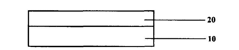
[0024] Step 1: If figure 1 As shown, a dielectric passivation layer 20 is deposited on the sample 10 to be prepared with a T-shaped gate. The thickness of the dielectric passivation layer 20 is 50-100 nm, and the material of the dielectric passivation layer 20 is silicon nitride, silicon dioxide or Aluminum oxide; the material of the sample 10 can be gallium nitride, arsenic nitride or indium phosphide and other group III and five semiconductors, and can also be silicon;

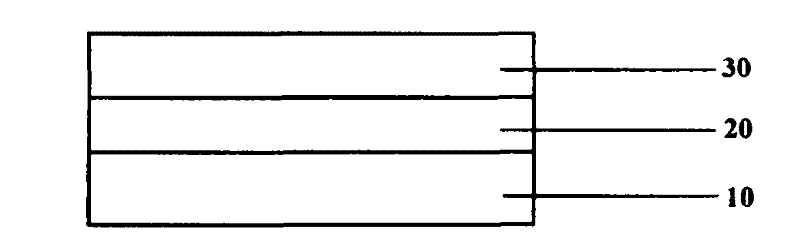
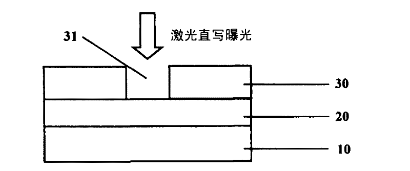
[0025] Step 2: If figure 2 As shown, a resist 30 is coated on the dielectric passivation layer 20, and the resist 30 is electron beam glue or ordinary ultraviolet photoresist; according to the size of the gate foot pattern 31 to be obtained, electron beam can be used. Glue (gate pattern, ≤0.1μm)...


PUM

PropertyMeasurementUnit
thicknessaaaaaaaaaa

Abstract

The invention relates to a semiconductor material and a device production field, especially to a method for producing a semiconductor T-shaped gate electrode by utilizing a photon beam super-diffraction technology. The method comprises the following steps: depositing a dielectric passivation layer on a sample on which a T-shaped gate is produced; then coating a resist, exposing, developing and fixing the resist by utilizing the photon beam super-diffraction nano-processing technology to form a gate foot pattern; then etching the dielectric passivation layer below the gate foot pattern by using the RIE (reactive ion etching) technology to form a groove; exposing, developing and fixing a photoresist by utilizing the photon beam super-diffraction nano-processing technology to form a gate head pattern, evaporating a gate metal, and forming a three-dimensional T-shaped metal electrode on the groove and the gate head pattern of the dielectric passivation layer. The invention has advantages of high flexibility, high precision, large area, repetition, low cost and high efficiency.

Description

technical field [0001] The invention relates to the field of semiconductor material and device manufacturing, in particular to a method for preparing a semiconductor T-shaped gate electrode by using photon beam super-diffraction technology. Background technique [0002] The so-called photon beam superdiffraction nanofabrication technology is an emerging femtosecond pulsed laser two-photon micro-nanofabrication technology that utilizes the two-photon effect and the threshold effect of the interaction between laser and matter. [0003] As one of the important advanced manufacturing technologies, laser processing technology has been widely used in many industrial manufacturing fields. When using laser direct writing technology for material processing, the processing resolution that can be achieved has been limited by the diffraction limit of classical optical theory, which is difficult to achieve. processing at the nanometer scale. The emergence of femtosecond pulsed laser not...

Claims


Application Information

Patent Timeline
Patent Type & Authority Patents(China)
IPC IPC(8): H01L21/28G03F7/00
Inventor 颜伟杜彦东韩伟华杨富华
Owner INST OF SEMICONDUCTORS - CHINESE ACAD OF SCI
Why Eureka
Try Eureka