High-performance semiconductor device and manufacturing method thereof

A technology of semiconductors and devices, which is applied in the field of high-performance semiconductor devices and their manufacturing, and can solve problems such as device performance degradation

Active Publication Date: 2011-08-17
INST OF MICROELECTRONICS CHINESE ACAD OF SCI
View PDF3 Cites 11 Cited by
  • Summary
  • Abstract
  • Description
  • Claims
  • Application Information

AI Technical Summary

Problems solved by technology

[0005] Both of the above two situations will cause the performance of the device to decrease. Therefore, it is necessary to propose a new semiconducto

Method used


Image

  • High-performance semiconductor device and manufacturing method thereof
  • High-performance semiconductor device and manufacturing method thereof
  • High-performance semiconductor device and manufacturing method thereof

Examples


no. 1 example

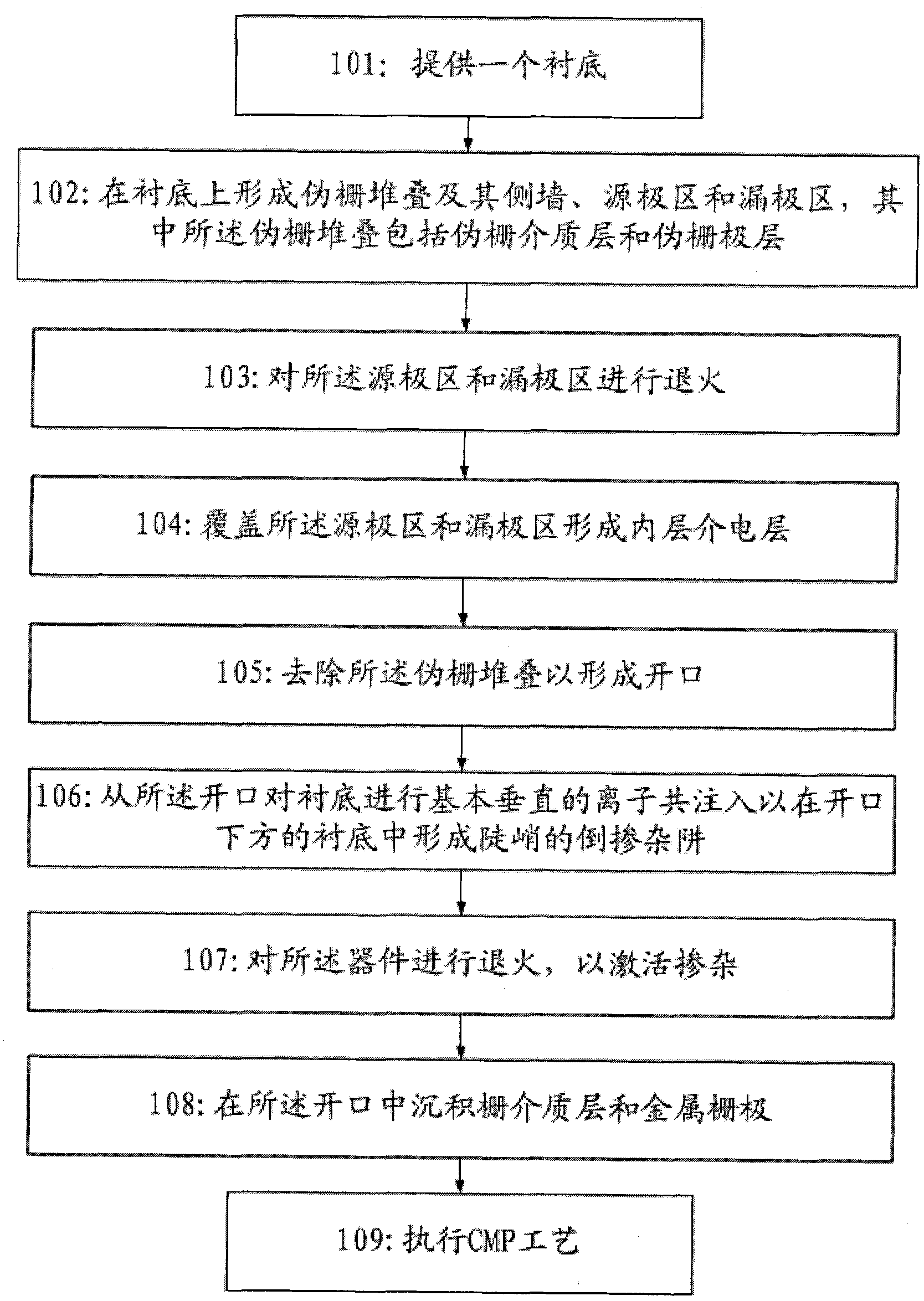
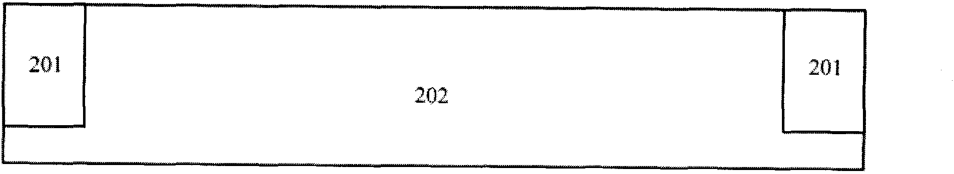
[0020] refer to figure 1 , figure 1 A flowchart showing a method of manufacturing a semiconductor device according to an embodiment of the present invention. In step 101, first provide a semiconductor substrate 202, refer to figure 2 . In this embodiment, the substrate 202 includes a silicon substrate (such as a wafer) in a crystal structure and an isolation region 201 . The substrate 202 may include various doping configurations according to design requirements known in the art (eg, p-type substrate or n-type substrate). Other example substrates 202 may also include other basic semiconductors, such as germanium and diamond. Alternatively, the substrate 202 may include a compound semiconductor, such as silicon carbide, gallium arsenide, indium arsenide, or indium phosphide. Furthermore, substrate 202 may optionally include epitaxial layers, may be altered by stress to enhance performance, and may include a silicon-on-insulator (SOI) structure.

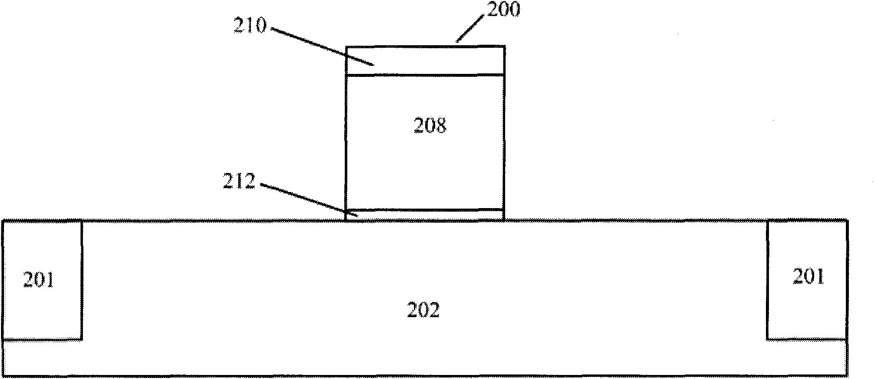
[0021] In step 102, as ...

no. 2 example

[0034] Only the aspects of the second embodiment that differs from the first embodiment will be described below. Parts not described should be considered to be performed by the same steps, methods or processes as those in the first embodiment, and thus will not be described again. In the flow chart according to the second implementation of the present invention such as Figure 12 as shown in Figure 12 As shown, in step 206 , the substrate 202 is co-implanted with oblique angle ions from the opening to form steep ion implantation regions 207 near the source region and the drain region respectively. The ion co-implantation depth range of the oblique angle is about 5-500nm. The co-implantation of ions at an oblique angle to the substrate 202 from the opening can be carried out in the following manner: performing the first oblique angle ion implantation, and implanting the first dopant into the substrate 202 to form the first dopant in the source region and the drain electrode ...

no. 3 example

[0038] Only the aspects of the third embodiment that differs from the first embodiment will be described below. Parts not described should be considered to be performed by the same steps, methods or processes as those in the first embodiment, and thus will not be described again. In the flow chart according to the third implementation of the present invention such as Figure 16 as shown in Figure 16 As shown, in step 306, substantially vertical ion co-implantation and oblique angle ion co-implantation are performed on the substrate 202 from the opening, thereby forming a steep retrograde well 206 in the substrate 202 below the opening and respectively Steep ion implantation regions 207 are formed near the source and drain regions 204 . The depth range of the substantially vertical ion co-implantation and oblique angle ion co-implantation is about 5-500 nm.

[0039] The substantially vertical ion co-implantation and oblique angle ion co-implantation can be performed in the ...


PUM

PropertyMeasurementUnit
Thicknessaaaaaaaaaa

Abstract

The invention provides a method for manufacturing a semiconductor device, comprising the following steps of: firstly forming a false gate stack and a side wall thereof, a source electrode region and a drain electrode region by utilizing a gate alternative process; annealing the source electrode region and the drain electrode region, and then removing the false gate stack; carrying out basically vertical ion co-implantation and/or slant ion co-implantation on a substrate to form a steep inverted dopant well in the substrate positioned below an opening and/or respectively form ion implantation regions near the source electrode region and the drain electrode region by utilizing the opening formed by removing the false gate stack, and then annealing the semiconductor device to activate doping; and depositing a gate dielectric layer and a metal gate electrode in the opening. Thus, the increase of tape-to-tape leakage currents and source drain junction capacitances of an MOSFET (Metal-Oxide-Semiconductor Field Effect Transistor) device are inhibited and the breakdown of a source electrode and a drain electrode is prevented, thereby the performance of the semiconductor device is improved.

Description

technical field [0001] The present invention generally relates to a semiconductor device and a method of manufacturing the same. More specifically, it relates to a semiconductor device and a method of manufacturing the same, which are used to form a steep doped well in a semiconductor substrate below a gate stack and in a semiconductor substrate near a source region and a drain region, respectively. A steep ion implantation region is formed. Background technique [0002] With the development of the semiconductor industry, integrated circuits with higher performance and more functions require greater component density, and the size, size and space of each component, between components, or each component itself needs to be further reduced. Correspondingly, in order to improve the performance of the MOSFET (Metal Oxide Semiconductor Field Effect Transistor) device, it is necessary to further reduce the gate length of the MOSFET device. However, as the gate length continues to...

Claims


Application Information

Patent Timeline
IPC IPC(8): H01L21/336H01L29/78
Inventor 骆志炯朱慧珑尹海洲
Owner INST OF MICROELECTRONICS CHINESE ACAD OF SCI
Why Eureka
Try Eureka