Low-power consumption bandwidth-multiplying operational amplifier realized by metal oxide semiconductor (MOS) devices

A technology of operational amplifiers and MOS devices, applied in the direction of DC coupled DC amplifiers, differential amplifiers, etc., can solve the problems of small signal current waste, difficulty in achieving high bandwidth performance, high static power consumption, etc., and achieve the effect of increasing low frequency gain

Active Publication Date: 2011-08-17
TSINGHUA UNIV
View PDF3 Cites 14 Cited by
  • Summary
  • Abstract
  • Description
  • Claims
  • Application Information

AI Technical Summary

Problems solved by technology

[0006] 1. Compared with other types of amplifiers, its static power consumption is high
[0007] 2. The current sources N1 and N2 are only used as current sources, and it is a "was

Method used


Image

  • Low-power consumption bandwidth-multiplying operational amplifier realized by metal oxide semiconductor (MOS) devices
  • Low-power consumption bandwidth-multiplying operational amplifier realized by metal oxide semiconductor (MOS) devices
  • Low-power consumption bandwidth-multiplying operational amplifier realized by metal oxide semiconductor (MOS) devices

Examples


Embodiment Construction

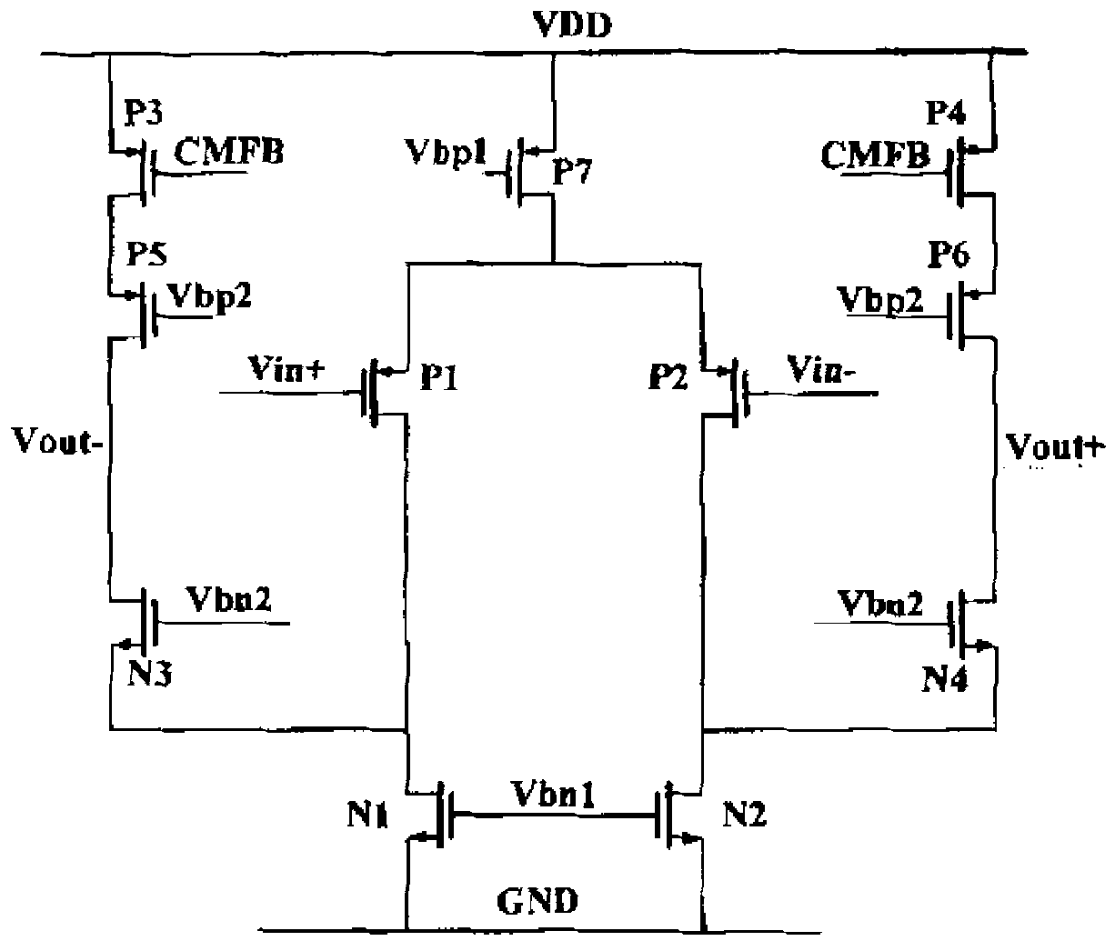
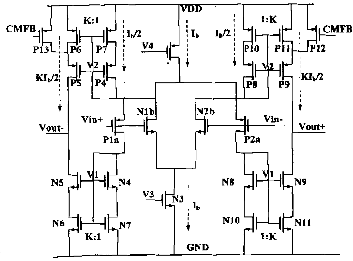
[0020] The present invention proposes a low-power consumption bandwidth multiplication operational amplifier realized by MOS devices, such as figure 2 As shown, it includes a shunt input stage, an intermediate stage for amplifying and recovering current, and a rail-to-rail output stage; the shunt input stage is mainly composed of PMOS transistors P1a, P2a and NMOS transistors N1b, N2b; the shunt input stage is composed of PMOS transistor P1a , P2a and NMOS transistors N1b, N2b; the intermediate stage of the amplification and recovery current is composed of four current mirrors, wherein NMOS transistors N4, N6, N7 form the first current mirror, and NMOS transistors N8, N10, N11 form the second current mirror Mirror, PMOS transistors P4, P6, P7 form the third current mirror, PMOS transistors P8, P10, P11 form the fourth current mirror; the rail-to-rail output stage is composed of NMOS transistors N5, N9 and PMOS transistors P5, P9.

[0021] exist figure 2 Among them, the posi...


PUM


Abstract

The invention discloses a low-power consumption bandwidth-multiplying operational amplifier realized by metal oxide semiconductor (MOS) devices, which belong to the field of analogue integrated circuit design. The amplifier comprises a shunting input stage, an intermediate stage and a rail-to-rail output stage, wherein the shunting input stage consists of two N-channel metal oxide semiconductor (NMOS) transistors and two P-channel metal oxide semiconductor (PMOS) transistors, converts an input voltage signal into a current signal, and forms low forward-backward signal current; the intermediate stage consists of four low voltage current mirrors, and amplifies recovery current to realize a recovery current amplification function; and the rail-to-rail output stage consists of four PMOS transistors and four NMOS transistors to realize the rail-to-rail output of signals. The low-power consumption bandwidth-multiplying operational amplifier has a plurality of advantages of capability of increasing a bandwidth by more than triple under the condition of not remarkably increasing power consumption, increasing of low frequency gain and signal swing rate, capability of working in a low voltage environment to increase input/output signal amplitude, and the like; each MOS device can adopt the conventional MOS transistors, and also can adopt strained silicon MOS devices with high mobility to further improve the performance of the circuit.

Description

technical field [0001] The invention belongs to the field of analog integrated circuit design. In particular, it relates to a novel low power bandwidth doubler operational amplifier. Background technique [0002] Since the 20th century, with the development of submicron and ultra-deep submicron technology and the increasing maturity of system chip technology, portable electronic products powered by batteries have achieved rapid development and rapid popularization. Since the development of battery technology is far behind the development of electronic systems, products ranging from heart pacemakers to hearing aids, mobile phones and various products have imposed strict restrictions on the supply voltage of electronic products. On the other hand, as the size of the device continues to shrink, the breakdown voltage of the process is also reduced, which also imposes strict restrictions on the power supply voltage. The performance requirements of electronic devices are getting...

Claims


Application Information

Patent Timeline
IPC IPC(8): H03F3/45
Inventor 方华军赵晓梁仁荣王敬许军
Owner TSINGHUA UNIV
Why Eureka
Try Eureka