Method for manufacturing groove type longitudinal semiconductor device

A manufacturing method and semiconductor technology, applied in semiconductor/solid-state device manufacturing, electrical components, circuits, etc., can solve the problems of difficulty in accurately controlling the height of silicon dioxide, increasing process complexity, and small process tolerance, achieving low cost, Improved dynamic characteristics, the effect of a simple method

Inactive Publication Date: 2011-09-14
UNIV OF ELECTRONICS SCI & TECH OF CHINA +1
View PDF3 Cites 15 Cited by
  • Summary
  • Abstract
  • Description
  • Claims
  • Application Information

AI Technical Summary

Problems solved by technology

However, after forming the active region (including the body region 5, the body contact region 7 and the source region 9), the process steps of small-tilt-angle ion implantation, oxide-filled extension trenches, and trench gate formation have the following main disadvantages: (1 ) process is difficult to accurately control the height of silicon dioxide in the first trench
On the one hand, the groove gate must span the body region in the vertical direction (that is, the upper surface of the oxide in the first trench cannot be higher than the lower surface of the body region); on the other hand, the longer the groove shed overlaps with the drift region, the gate-drain The greater the capacitance, and the withstand voltage of the device decreases with the decrease of the height of silicon dioxide in the first trench, so the height of silicon dioxide in the first trench needs to be accurately controlled in the process to ensure the electrical performance of the device; (2) the device The higher the withstand voltage, the deeper the first trench, the more difficult the implantation, and the smaller the process tolerance; (3) In order to ensure that the ions implanted at a small inclination angle cover all areas below the active layer on both side walls of the trench, and do not cover the trench Active layer on both side walls, mask for ion implantation ( image 3 13 is the mask) is more difficult to do, increasing the complexity of the process

Method used


Image

  • Method for manufacturing groove type longitudinal semiconductor device
  • Method for manufacturing groove type longitudinal semiconductor device
  • Method for manufacturing groove type longitudinal semiconductor device

Examples


Embodiment 1

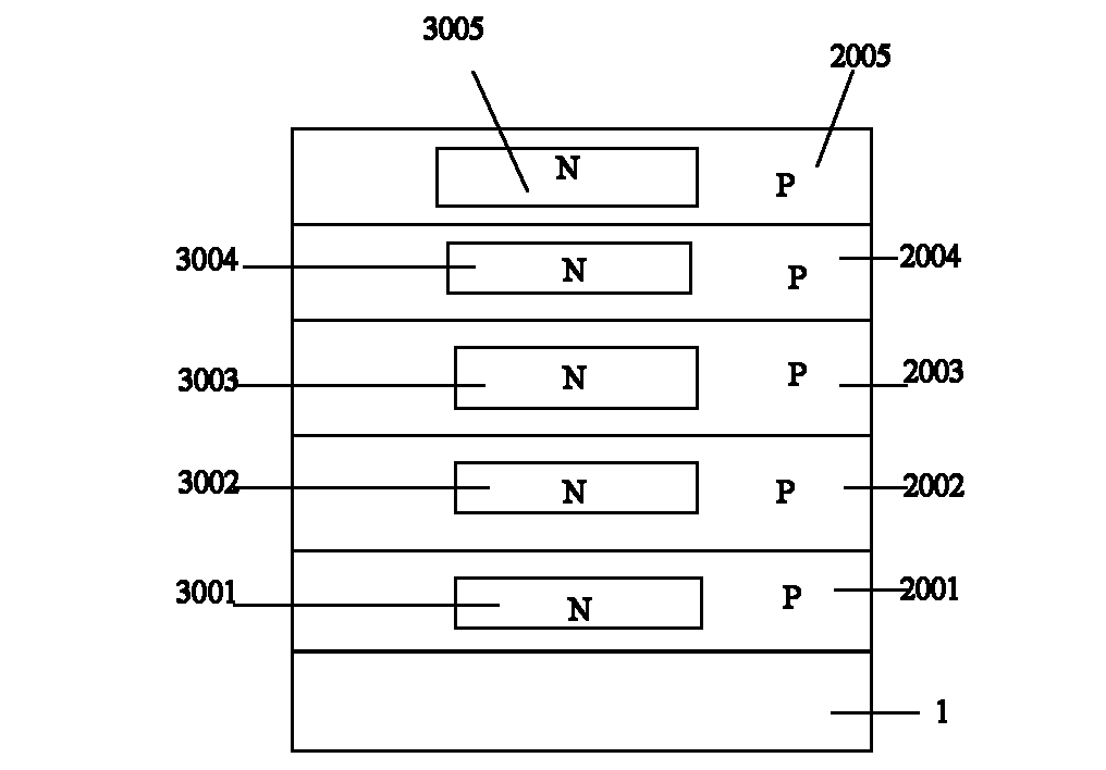
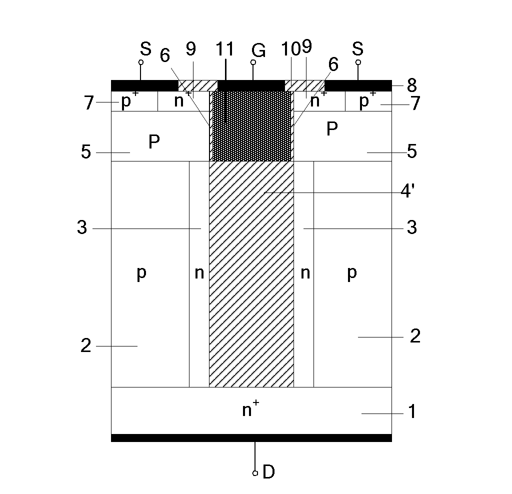
[0067] As a preferred embodiment of the present invention, the present invention discloses a novel superjunction semiconductor device structure (such as Figure 4h Shown) the manufacture method, it comprises the steps:

[0068] a, in the semiconductor substrate 1 (in this embodiment is n + epitaxially forming a first semiconductor drift region 2 on a type semiconductor substrate);

[0069] b. On the first semiconductor drift region 2, partially etch the first semiconductor drift region 2 up to the semiconductor substrate to form a first trench, such as Figure 4a shown.

[0070] c. Growing a diffusion mask layer 14 on the back side of the semiconductor substrate and the top of the first semiconductor drift region 2, such as Figure 4b Shown; impurity diffusion and annealing are then performed to form the second semiconductor drift region 3 on the trench wall; the diffusion masking layer 14 is removed, as Figure 4cshown; the first semiconductor drift region and the second ...

Embodiment 2

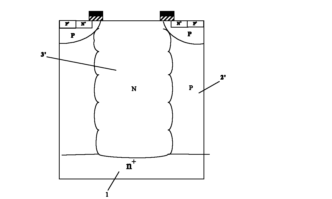
[0084] The manufacturing process of the semiconductor device of the present invention described in Embodiment 1 is preferably applied to a MOS control vertical device, so as to alleviate the contradictory relationship among withstand voltage, on-resistance and switching loss. Applied in such as Figure 5a when the IGBT device shown. The difference from Example 1 is that the initial semiconductor material substrate 1 is P + The conductivity type of the semiconductor substrate 101 is the same as that of the first semiconductor drift region. Its key steps are as Figure 5b and Figure 5c shown. All the other steps are identical to Example 1.

Embodiment 3

[0086] The manufacturing process of the semiconductor device of the present invention described in Embodiment 1 can be applied to control vertical devices of N-channel MOS, and can also be applied to control vertical devices of P-channel MOS. P-channel VDMOS as Figure 6a shown. When used in the manufacture of P-channel MOS control vertical devices, the semiconductor substrate 1, the first semiconductor drift region 2, the second semiconductor drift region 3 formed by diffusion, the active region 5, the body contact region 7, the source region 9 and the N The channel MOS controls the doping type of the corresponding region of the vertical device. The key steps are as follows: Figure 6b and Figure 6c shown. In Embodiment 1, an N-channel VDMOS is manufactured, and N-type impurities are diffused on the trench sidewall of the P-type first semiconductor drift region 2 to form a second semiconductor drift region 3; in this embodiment, a P-channel VDMOS is manufactured, The sec...


PUM


Abstract

The invention discloses a method for manufacturing a groove type longitudinal semiconductor device, belonging to the technical field of manufacture of semiconductor devices. In the invention, the process manufacturing of the groove type longitudinal semiconductor device can be realized through the process steps such as deep groove etching, high-temperature diffusion, insulating medium padding and planarization, active layer and electrode forming and the like. Compared with the existing process, the process method disclosed by the invention has the following advantages: firstly, a narrow and high-concentration P column region or N column region (namely a second semiconductor drift region) are be formed, thereby being beneficial to reduction of on resistance and decrease of horizontal dimension of the device; secondly, the bottom of a groove grid is ensured to be parallel to the lower interface of a body region or be slightly lower than the lower interface of the body region, further improving the withstand voltage of the device and reducing the low-grid and grid-drain capacitance; and thirdly, complicated masking is not required, and the influence of small-angle injection to the channel region can be avoided; and fourthly, the negative influence on the formed body region, body contact region and source region caused by the padding and planarization of the extended groove as well as manufacturing and planarization of the groove grid can be avoided.

Description

technical field [0001] The invention belongs to the technical field of semiconductor device manufacturing, and in particular relates to a method for manufacturing a semiconductor device with deep grooves. Background technique [0002] Power MOSFET is a multi-subconduction device, which has many advantages such as high input impedance, high frequency, and positive temperature coefficient of on-resistance. These advantages make it widely used in the field of power electronics, greatly improving the efficiency of electronic systems. [0003] The high voltage resistance of the device requires a long drift region and a low doping concentration in the drift region. However, as the length of the drift region increases and the doping concentration decreases, the on-resistance (R on ) increases, the on-state power consumption increases, and the device on-resistance R on There is the following relationship with the breakdown voltage BV: that is, R on ∝BV 2.5 . [0004] With the ...

Claims


Application Information

Patent Timeline
Patent Type & Authority Applications(China)
IPC IPC(8): H01L21/336
Inventor 罗小蓉王元刚姚国亮雷天飞葛瑞陈曦张波李肇基
Owner UNIV OF ELECTRONICS SCI & TECH OF CHINA
Why Eureka
Try Eureka