Manufacturing method of cold metal oxide semiconductor (MOS) super-junction structure and cold MOS super-junction structure

A manufacturing method and N-type technology, applied in semiconductor/solid-state device manufacturing, electrical components, circuits, etc., can solve the problems of uneven bonding surface of super junction structure, and achieve the goal of overcoming uneven bonding surface, good controllability, reducing The effect of manufacturing cost

Inactive Publication Date: 2011-09-14
ADVANCED SEMICON MFG CO LTD
View PDF10 Cites 9 Cited by
  • Summary
  • Abstract
  • Description
  • Claims
  • Application Information

AI Technical Summary

Problems solved by technology

[0007] The technical problem to be solved by the present invention is to provide a method for manufacturing a cold MOS superjunction structure and a cold MOS superjunction structure, which can avoid the need for multiple photolithography, ion implantation, push and epitaxy in the preparation of traditional superjunction structures. Growth and other complex processes effectively reduce manufacturing costs and overcome the shortcomings of the traditional "candied haws"-shaped super-junction structure with uneven joint surfaces

Method used


Image

  • Manufacturing method of cold metal oxide semiconductor (MOS) super-junction structure and cold MOS super-junction structure
  • Manufacturing method of cold metal oxide semiconductor (MOS) super-junction structure and cold MOS super-junction structure
  • Manufacturing method of cold metal oxide semiconductor (MOS) super-junction structure and cold MOS super-junction structure

Examples


Embodiment Construction

[0030] The present invention will be further described below in conjunction with specific embodiments and accompanying drawings, but the protection scope of the present invention should not be limited thereby.

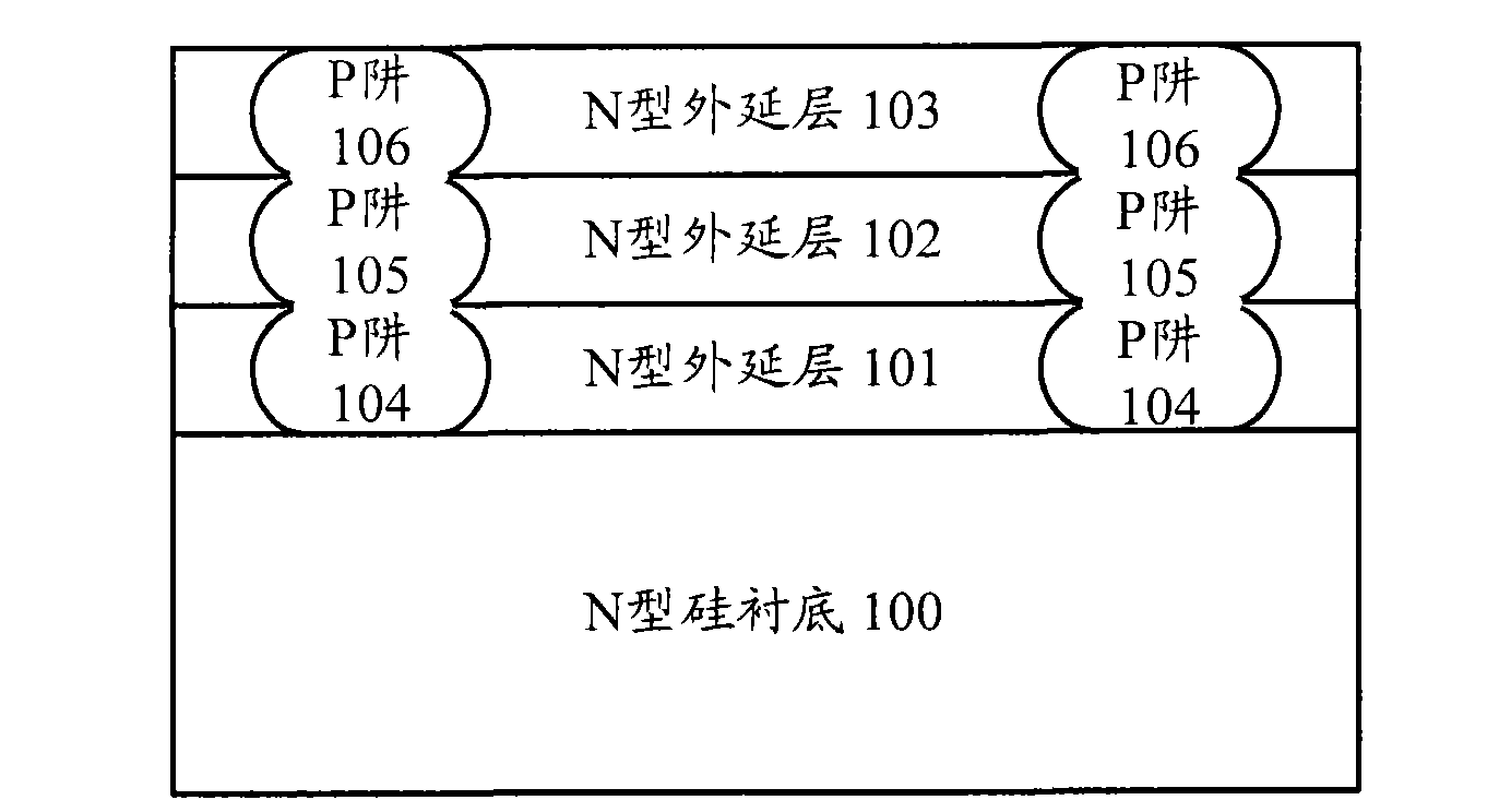
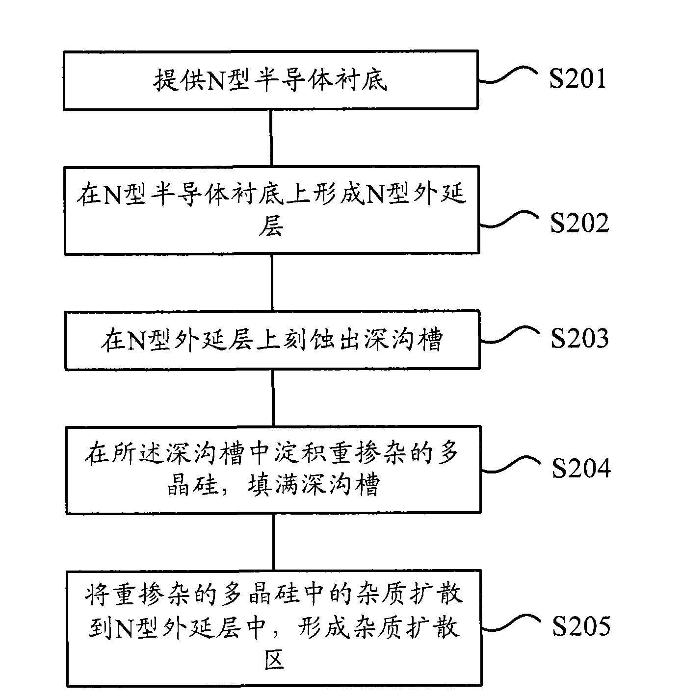
[0031] figure 2 It is a flowchart of a method for manufacturing a cold MOS super junction structure according to an embodiment of the present invention. As shown in the figure, the manufacturing method starts at step S201. The method may include: performing step S201, providing an N-type semiconductor substrate; performing step S202, forming an N-type epitaxial layer on the N-type semiconductor substrate; performing step S203, etching a deep trench on the N-type epitaxial layer; Step S204 is executed to deposit heavily doped polysilicon in the deep trench to fill up the deep trench; step S204 is executed to diffuse impurities in the heavily doped polysilicon into the N-type epitaxial layer to form an impurity diffusion region.

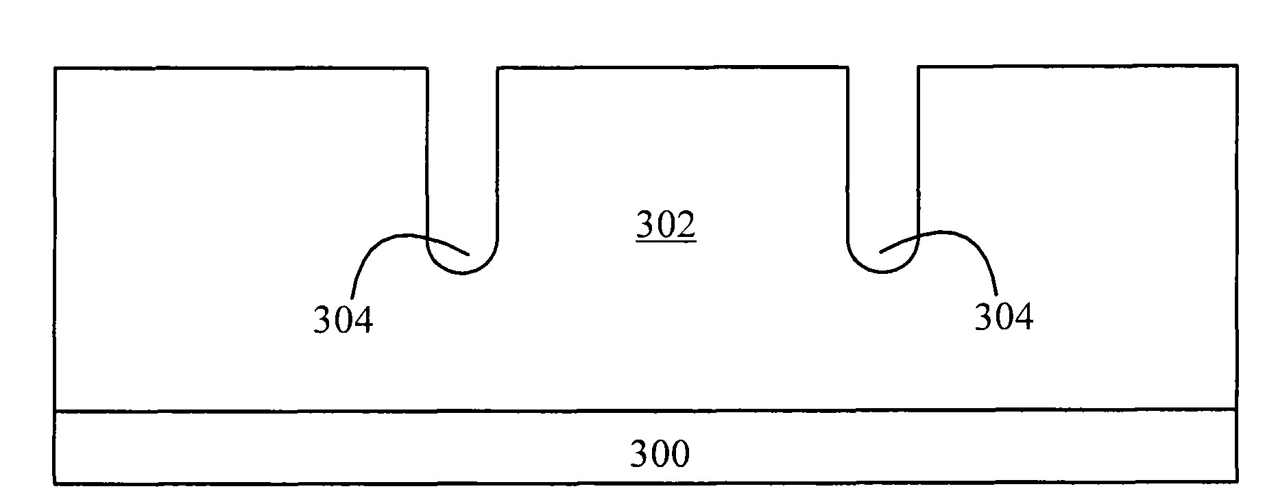
[0032] Figure 3 to Figure 5 It is a...


PUM

PropertyMeasurementUnit
widthaaaaaaaaaa
depthaaaaaaaaaa
depthaaaaaaaaaa

Abstract

The invention provides a manufacturing method of a cold metal oxide semiconductor (MOS) super-junction structure. The method comprises the following steps of: providing an N type semiconductor substrate; forming an N type epitaxial layer on the N type semiconductor substrate; etching a deep groove on the N type epitaxial layer; depositing heavily doped polysilicon in the deep groove, and fully filling the deep groove; and diffusing impurities in the heavily doped polysilicon into the N type epitaxial layer to form an impurity diffusing area. Correspondingly, the invention also provides the cold MOS super-junction structure. The cold MOS super-junction structure is manufactured through a deep groove etching technology, so complex processes, such as photoetching for multiple times, ion implantation, propelling, epitaxial growth and the like, required in the preparation of the traditional super-junction structure are avoided, the manufacturing cost is effectively reduced, and the defect that electricity leakage is easy to cause when an MOS device works because the joint face of the traditional super-junction structure which is in a shape like sugarcoated haws on a stick is not uniform. By the method, the breakdown voltage of the MOS device can be effectively increased, the on resistance of the MOS device can be greatly reduced, the process is simple, and the controllability is high.

Description

technical field [0001] The invention relates to the technical field of semiconductor manufacturing, in particular, the invention relates to a method for manufacturing a cold MOS super junction structure and a cold MOS super junction structure. Background technique [0002] Power MOSFET is widely used in medium and low voltage due to its high input impedance, low loss, fast switching speed, no secondary breakdown, wide safe working area, good dynamic performance, easy coupling with the front pole to achieve large current, and high conversion efficiency. power conversion and control field. Although power MOS devices have been amazingly improved in terms of power handling capability, in the high-voltage field due to the on-resistance Ron, the conduction loss of power MOS devices increases rapidly with the increase of withstand voltage. In order to improve withstand voltage and reduce conduction loss, a series of new structures and technologies have emerged. Among them, the su...

Claims


Application Information

Patent Timeline
Patent Type & Authority Applications(China)
IPC IPC(8): H01L21/336H01L29/78H01L29/06
Inventor 永福陈雪萌龚大卫
Owner ADVANCED SEMICON MFG CO LTD
Why Eureka
Try Eureka