Ultraviolet avalanche diode imaging array pixel, application method thereof and avalanche transistor imaging array

An imaging array and application method technology, applied in the direction of radiation control devices, etc., can solve the problems of high defect density, low yield, difficult manufacturing of GaN and AlGaN avalanche tubes, etc., and achieve the effect of increasing the photosensitive area and improving the yield

Active Publication Date: 2011-09-14
NANJING UNIV
View PDF6 Cites 1 Cited by
  • Summary
  • Abstract
  • Description
  • Claims
  • Application Information

AI Technical Summary

Problems solved by technology

[0005] As mentioned earlier, due to the lattice dislocation of GaN and AlGaN materials, the defect density is very high, GaN and AlGa

Method used


Image

  • Ultraviolet avalanche diode imaging array pixel, application method thereof and avalanche transistor imaging array
  • Ultraviolet avalanche diode imaging array pixel, application method thereof and avalanche transistor imaging array
  • Ultraviolet avalanche diode imaging array pixel, application method thereof and avalanche transistor imaging array

Examples


Embodiment Construction

[0050] Such as Figure 3A Shown is a schematic diagram of the imaging array pixel of the ultraviolet avalanche tube of the present invention.

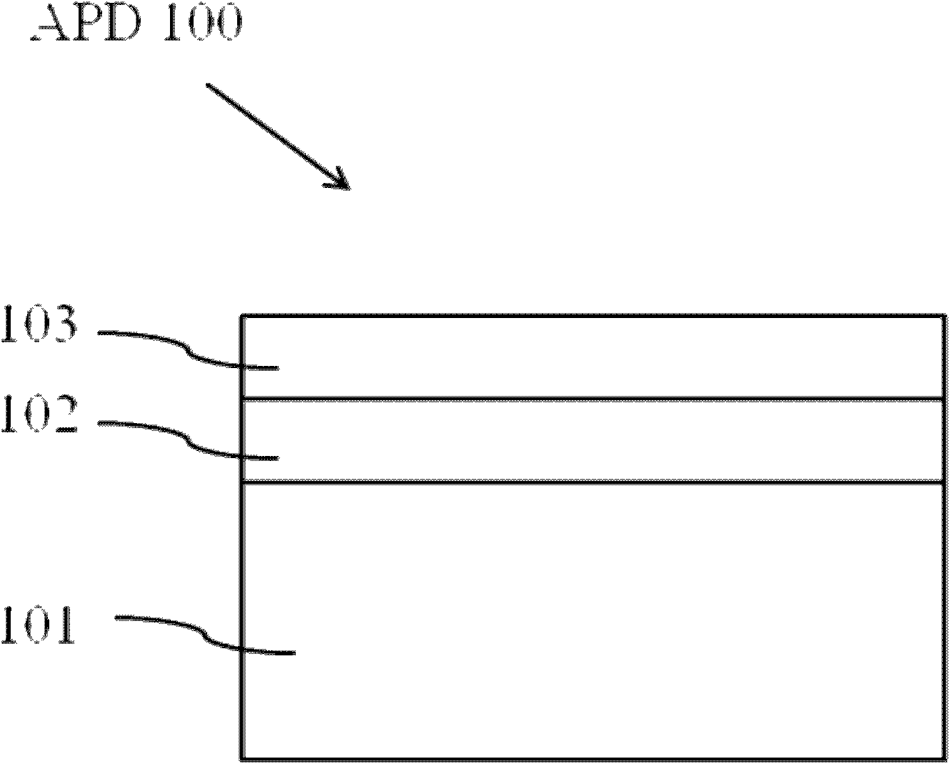
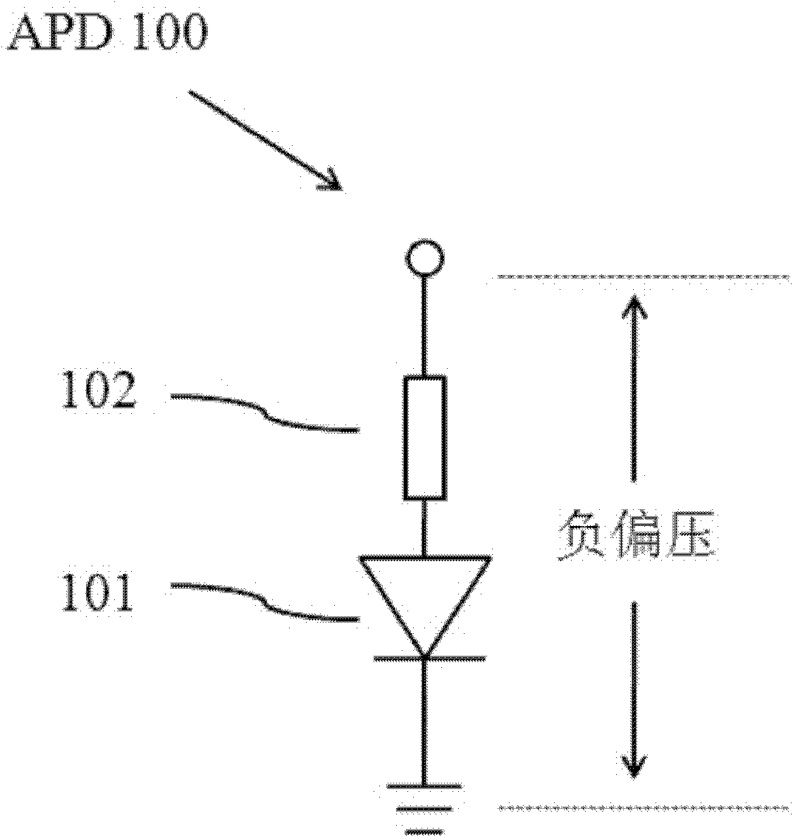
[0051] If the ultraviolet avalanche tube imaging array pixel UV-APD 300 is composed of a plurality of basic units UV-APD 200 (such as Figure 3B ) in parallel configuration, the radius of the UV-APD 200 can be 1 μm to 50 μm. exist Figure 3B Among them, we can form the substrate 201 from bottom to top. The substrate 201 can be made of materials such as SiC, sapphire, and silicon substrates, but the substrate is required to be transparent; the materials of the n-type semiconductor 202 and the p-type semiconductor 204 can be GaN, For materials such as AlN and AlGaN, n-type semiconductor 202 and p-type semiconductor 204 can be epitaxially grown by MOCVD, which also has a buffer layer, thereby reducing lattice dislocations in the material and reducing defect density; then etching the p-type semiconductor to expose Part of the n-type sem...


PUM

PropertyMeasurementUnit
Radiusaaaaaaaaaa
Resistanceaaaaaaaaaa

Abstract

The invention relates to an ultraviolet avalanche diode imaging array pixel, an application method thereof and an avalanche diode imaging array comprising the same. The ultraviolet avalanche diode imaging array pixel comprises a plurality of avalanche diode detectors which are connected in parallel; each avalanche diode detector comprises a photodiode, a film resistor and a metal layer which are orderly connected; and in each avalanche diode detector, an n-type semiconductor of the photodiode and a contact electrode are connected, electric connection is formed among the contact electrodes of all the avalanche diode detectors in the imaging pixel to serve as an electrode, an intact metal layer is shared by all the avalanche diode detectors and another electrode of the ultraviolet avalanchediode imaging array pixel is formed by the metal layer. The avalanche diode imaging array is composed of a plurality of ultraviolet avalanche diode imaging array pixels. The ultraviolet avalanche diode imaging array pixel disclosed by the invention has the effective effects that: the problem of too low yield caused by big defect density of a material per se is overcome and the yield of the ultraviolet avalanche diode imaging array pixel with a novel structure can approach and reach to 100%.

Description

technical field [0001] The invention relates to an ultraviolet light avalanche tube imaging array pixel, its application method and an avalanche tube imaging array. Background technique [0002] The detection of ultraviolet light, especially the solar-blind ultraviolet band, has extremely important applications in space detection and military affairs. At present, the photon counting system in the ultraviolet band uses a photomultiplier tube (PMT), but the photomultiplier tube is large in size, fragile, high in operating voltage and expensive, so a solid-state ultraviolet detector with a small size and cheap price is very important. The advantages. [0003] In recent years, with the advancement of GaN and AlGaN material technology, there have also been reports of GaN-based and AlGaN-based materials in the laboratory, such as ultraviolet avalanche tubes and single photon detection avalanche tubes (SPAD). However, due to the lattice dislocation of GaN and AlGaN materials them...

Claims


Application Information

Patent Timeline
IPC IPC(8): H01L27/146
Inventor 吴福伟闫锋
Owner NANJING UNIV
Why Eureka
Try Eureka