Bootstrapping sampling switch applied to high-speed and high-linearity analog-to-digital converter

An analog-to-digital converter, high linearity technology, applied in the direction of electronic switches, electrical analog memories, instruments, etc., can solve the problems of long off time and open time, limit the speed of switch switching, etc., and achieve simple structure and high switching speed The effect of high speed and low power consumption

Inactive Publication Date: 2011-09-14
BEIJING UNIV OF TECH
View PDF0 Cites 18 Cited by
  • Summary
  • Abstract
  • Description
  • Claims
  • Application Information

AI Technical Summary

Problems solved by technology

This kind of bootstrap switch has the disadvantage of long turn-off time and turn-on time, and the high-voltage NMOS tube (such as image 3 M11 and M12 in ) further limit the switching speed of the switch

Method used


Image

  • Bootstrapping sampling switch applied to high-speed and high-linearity analog-to-digital converter
  • Bootstrapping sampling switch applied to high-speed and high-linearity analog-to-digital converter
  • Bootstrapping sampling switch applied to high-speed and high-linearity analog-to-digital converter

Examples


Embodiment Construction

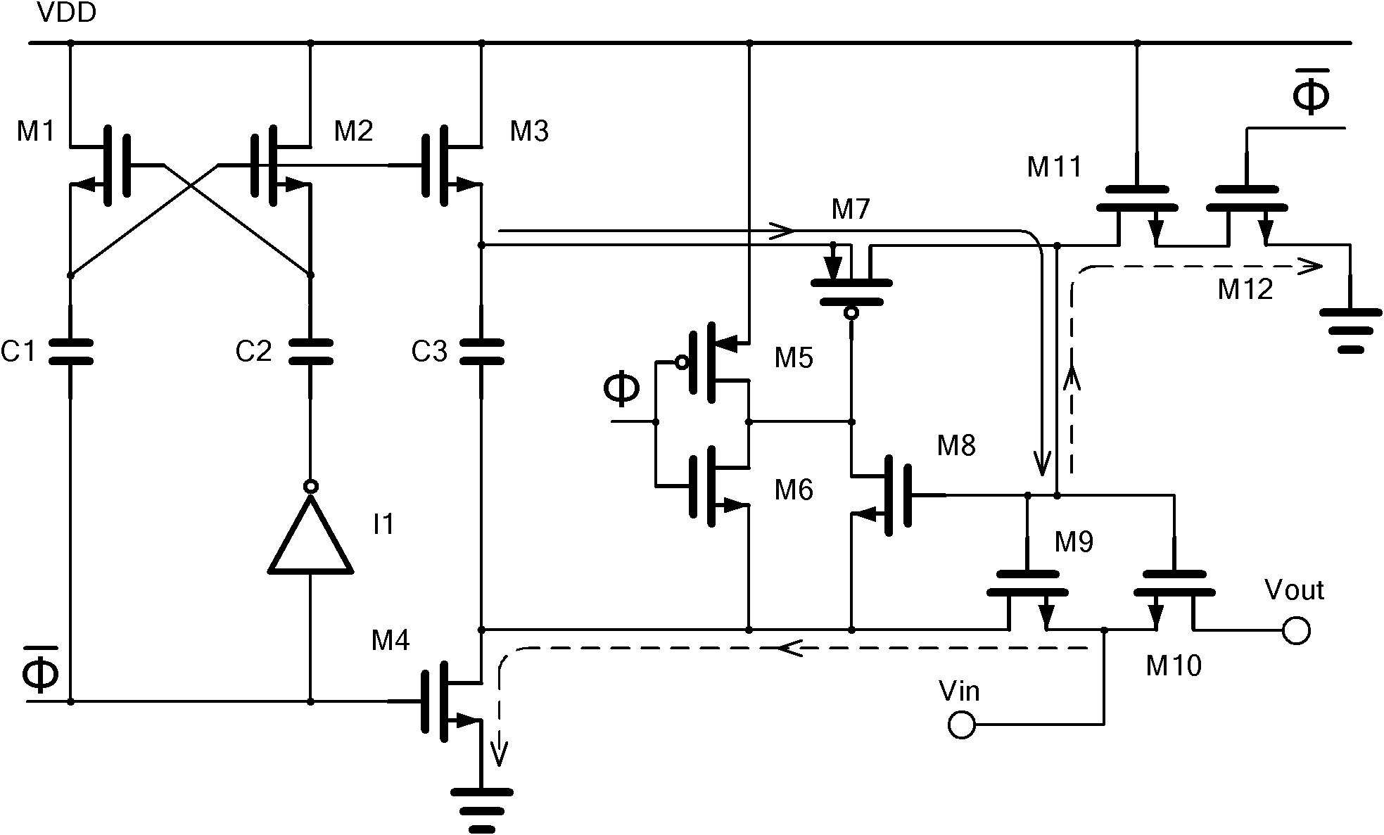
[0023] The bootstrap sampling switch in the embodiment of the present invention is as Figure 4 shown. Including: clock booster, gate-source voltage follower, conduction switch and charge-discharge enhancement circuit.

[0024] 1. The clock signal controls the bootstrap sampling switch from turn-off to turn-on:

[0025] The two NMOS transistors M6 and M13 are turned on at the same time, so that the gates of the three NMOS transistors M8, M9 and M10 can be charged before the PMOS transistor M7 is turned on. Since this part of the charging charge comes directly from the power supply instead of the capacitor C3, more charge can be added between the gate and source of the NMOS transistor M10 as a turn-on switch, corresponding to a higher gate-source voltage and lower on-resistance. In addition, a higher gate-source voltage can also speed up the turn-on speed of the two NMOS transistors M8 and M9, and indirectly speed up the turn-on speed of the PMOS transistor M7. When the PMO...


PUM


Abstract

The invention provides a bootstrapping sampling switch applied to a high-speed and high-linearity analog-to-digital converter. The bootstrapping sampling switch comprises a clock booster, a grid-source voltage follower, a conduction switch and a charging and discharging enhanced circuit, wherein several times of power voltage are generated by the clock booster and used for charging a capacitor; the grid-source voltage follower connects the capacitor between the grid and the source when the conduction switch is off, so that a relevantly constant grid-source voltage difference under different voltage input is ensured; the charging and discharging enhanced circuit is added in a charging or discharging loop during switching of the switch so as to shorten the off and on time, reduce a parasitic capacitance of the grid of the conduction switch and reduce the loss of the storage charge of the capacitor; the use of a high-voltage metal oxide semiconductor (MOS) tube is not needed; meanwhile, high-linearity sampling is realized (the sampling rate is more than 1 KMHz under 65-nano complementary metal-oxide-semiconductor (CMOS) technology and a stray-free dynamic range more than 95 decibels can be obtained). A complicated logic control circuit is absent in the structure, so the area of a chip cannot be increased; moreover, a requirement of the clock buffer is not needed to be enhanced.

Description

technical field [0001] The invention relates to an important module applied to a sample-and-hold circuit, in particular to an analog switch suitable for a high-speed, high-linearity analog-to-digital converter using bootstrapped and multiple charging and discharging path technologies. technical background [0002] In modern mixed-signal integrated circuits, the analog-to-digital converter is an indispensable part, and its conversion accuracy and speed play a decisive role in the performance of the whole system. The analog switches used in the sample-and-hold circuit determine the dynamic range and sampling rate of the ADC. [0003] figure 1 A simple sample-and-hold circuit composed of CMOS switches and capacitors is given. Traditional CMOS switches are difficult to be used in high-linearity analog-to-digital converters due to their large on-resistance and variations with the input signal (such as figure 2 shown as the green curve). Increasing the size of the MOS tube ca...

Claims


Application Information

Patent Timeline
Patent Type & Authority Applications(China)
IPC IPC(8): H03K17/687
CPCG11C27/024
Inventor 黄冠中林平分
Owner BEIJING UNIV OF TECH
Why Eureka
Try Eureka