Removal of a sheet from a production apparatus

A technology for plates and cooling plates, applied in the field of forming plates from melts

Inactive Publication Date: 2013-05-08
VARIAN SEMICON EQUIP ASSOC INC
View PDF3 Cites 0 Cited by
  • Summary
  • Abstract
  • Description
  • Claims
  • Application Information

AI Technical Summary

Problems solved by technology

Therefore, temperature variations along the sheet limit the usable width and thickness of the sheet

Method used


Image

  • Removal of a sheet from a production apparatus
  • Removal of a sheet from a production apparatus
  • Removal of a sheet from a production apparatus

Examples


Embodiment Construction

[0022] Embodiments of the devices and methods herein are described in connection with solar cells. However, such embodiments may also be used in the fabrication of, for example, integrated circuits, flat panels, or other substrates known to those skilled in the art. Additionally, although the melt is described herein as silicon, the melt may contain germanium, silicon and germanium, or other materials known to those skilled in the art. Accordingly, the invention is not limited to the specific examples described below.

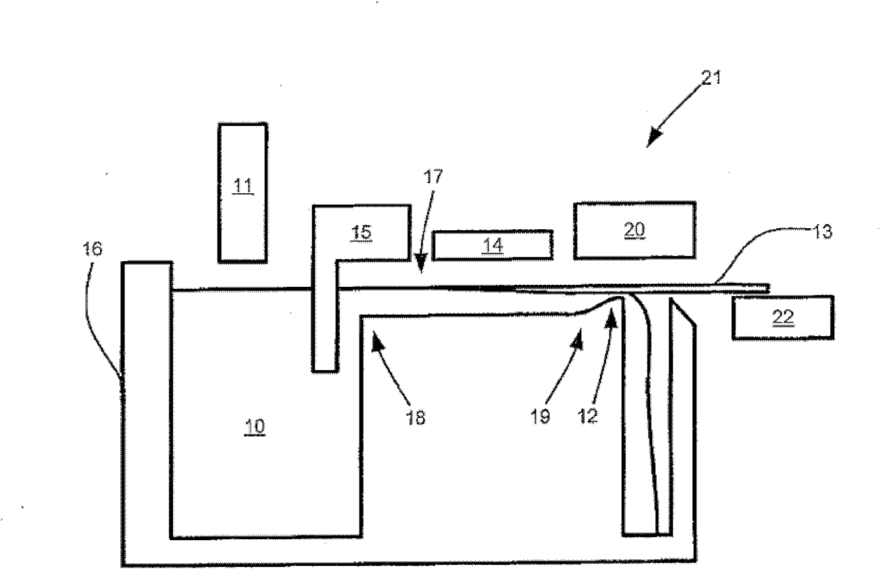
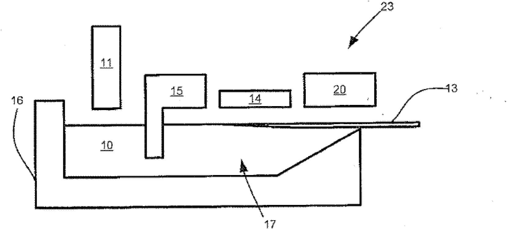
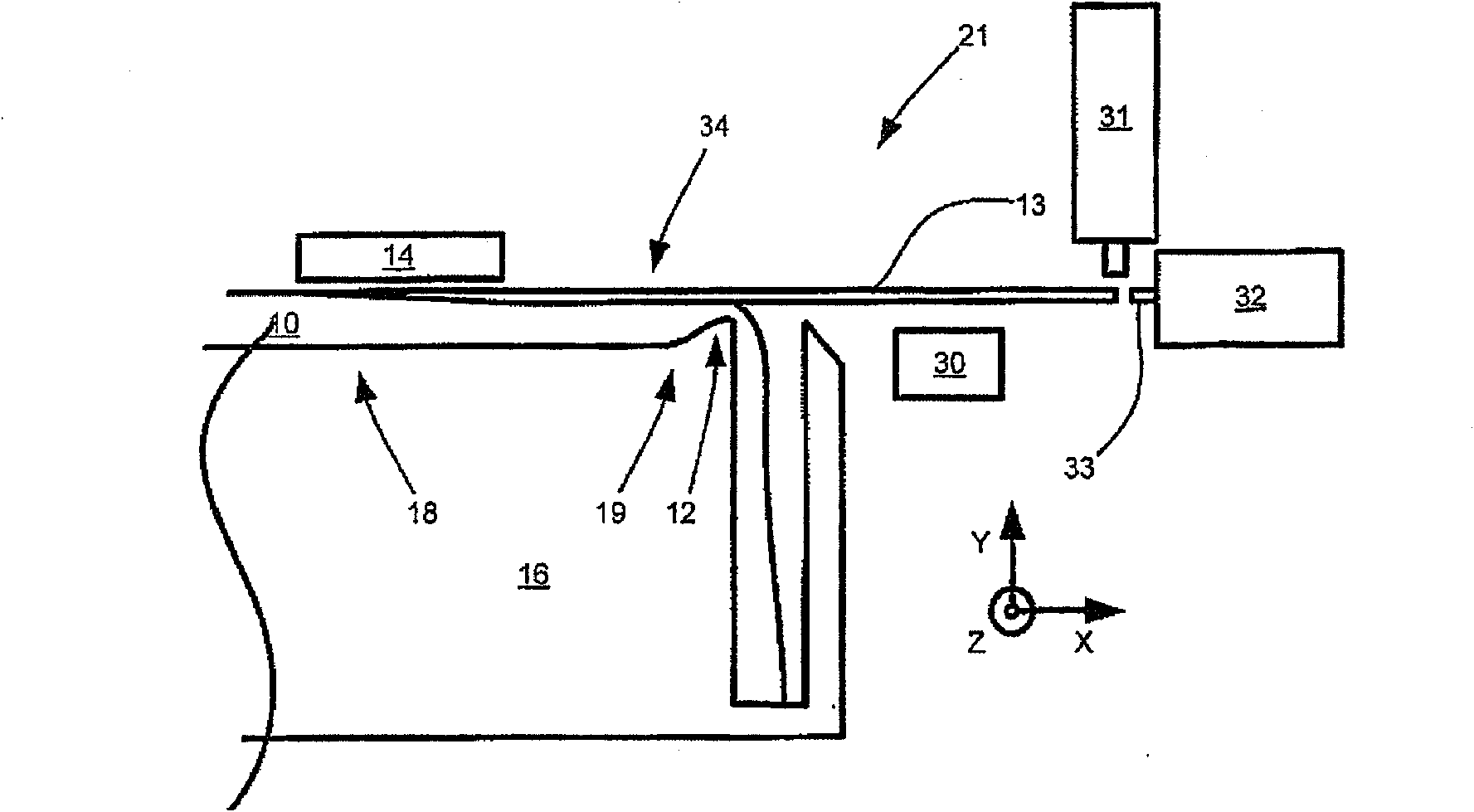
[0023] figure 1 Is a cross-sectional side view of one embodiment of an apparatus for separating sheet material from a melt. The device 21 for forming a plate has a container 16 and flat plates 15 and 20 . Container 16 and plates 15 and 20 may be, for example, tungsten, boron nitride, aluminum nitride, molybdenum, graphite, silicon carbide, or quartz. Vessel 16 is configured to contain melt 10 . Melt 10 may be silicon. In one embodiment, the melt 10 can b...


PUM

PropertyMeasurementUnit
thicknessaaaaaaaaaa

Abstract

A melt of a material is cooled and a sheet of the material is formed in the melt. This sheet is transported, cut into at least one segment, and cooled in a cooling chamber. The material may be Si, Si and Ge, Ga, or GaN. The cooling is configured to prevent stress or strain to the segment. In one instance, the cooling chamber has gas cooling.

Description

technical field [0001] The present invention relates to a method of forming a sheet from a melt, and in particular to a method of minimizing thermal stress on a sheet formed from a melt. Background technique [0002] For example, silicon wafers or panels may be used in the integrated circuit or solar cell industries. As the demand for renewable energy increases, the demand for solar cells continues to increase. Most solar cells are made from silicon wafers, such as single crystal silicon wafers. Currently, the major cost of crystalline silicon solar cells is the wafer on which the solar cells are fabricated. The efficiency of a solar cell, or the amount of power generated under standard lighting, is limited in part by the quality of the wafer. As the demand for solar cells increases, one goal of the solar cell industry is to reduce the cost / power ratio. Any reduction in the cost of manufacturing wafers without sacrificing quality will reduce the cost / power ratio and all...

Claims


Application Information

Patent Timeline
Patent Type & Authority Patents(China)
IPC IPC(8): H01L31/042H01L21/20
CPCC30B28/06H01L31/182Y10S588/90C30B29/06C30B29/403C30B29/60Y02E10/546C30B29/02C30B11/003C30B29/08C30B11/001C30B29/64Y02E10/50Y10T117/1024Y10T117/1092Y02P70/50H01L21/20H01L31/04H01L31/18
Inventor 彼德·L·凯勒曼菲德梨克·卡尔森法兰克·辛克莱
Owner VARIAN SEMICON EQUIP ASSOC INC
Why Eureka
Try Eureka