AC type plasma display element
A display element and plasma technology, applied in the field of lighting, can solve the problems of reduced product yield and increased manufacturing process costs, and achieve the effects of excellent discharge characteristics, reduced discharge voltage, and low working voltage
- Summary
- Abstract
- Description
- Claims
- Application Information
AI Technical Summary
Problems solved by technology
Method used
Image
Examples
Embodiment 1
[0070] Use CaO getter powder with an average particle size of 1 μm or less to coat the adsorption layer with a thickness of 2 μm or less, and apply a phosphor paste on its surface by printing to form a back substrate, which will have a crystalline binary system (Ca 0.15 Mg 0.85 ) The front substrate of the O oxide protective film and the above-mentioned rear substrate were fired at a temperature of 500° C., sealed in a nitrogen atmosphere, and then exhausted by heating and filled with a discharge gas to produce a PDP. Other conditions are the same as in Comparative Example 1.
experiment example 1
[0072] The discharge voltages of the respective PDPs produced in Comparative Examples 1 and 2 and the Examples were measured according to the aging time of the PDPs, and the results are shown in a graph. Figure 7 and Figure 8 middle.
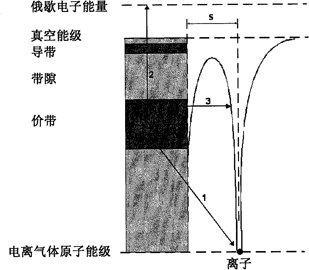
[0073] First, if Figure 7 As shown, in Comparative Example 1, the binary system (Ca 0.1 5Mg 0.85 The discharge voltage of the )O oxide protective film is about 305V, which is about 40V lower than the discharge voltage of the MgO protective film of Comparative Example 2, which is 345V. The reason for this drop in discharge voltage can be considered to be the binary system (Ca 0.15 Mg 0.85 ) The band gap energy of the O oxide protective film is reduced compared with that of MgO, thus increasing the secondary electron emission coefficient.
[0074] Next, if Figure 8 As shown, the PDP discharge voltage of embodiment 1 is reduced to 230V. In contrast, in the case of Comparative Example 2 using a protective film formed of MgO, the discharg...
PUM
| Property | Measurement | Unit |
|---|---|---|
| The average particle size | aaaaa | aaaaa |
| Thickness | aaaaa | aaaaa |
Abstract
Description
Claims
Application Information


