Plasma processing apparatus

A plasma and processing device technology, which is applied in the field of plasma processing devices, can solve problems such as excessive acceleration, defect formation, and disordered arrangement, and achieve the effect of improving characteristics

Inactive Publication Date: 2011-09-28
EBATEKKU
View PDF5 Cites 5 Cited by
  • Summary
  • Abstract
  • Description
  • Claims
  • Application Information

AI Technical Summary

Problems solved by technology

Moreover, these undesired atomic groups are deposited on the surface of the substrate, and there is a possibility that the quality of the silicon film will be reduced.
[0013] In addition, in the device described in Patent Document 2, since an electric field for accelerating ions is formed in the entire plasma generatio

Method used


Image

  • Plasma processing apparatus
  • Plasma processing apparatus
  • Plasma processing apparatus

Examples


Embodiment 1

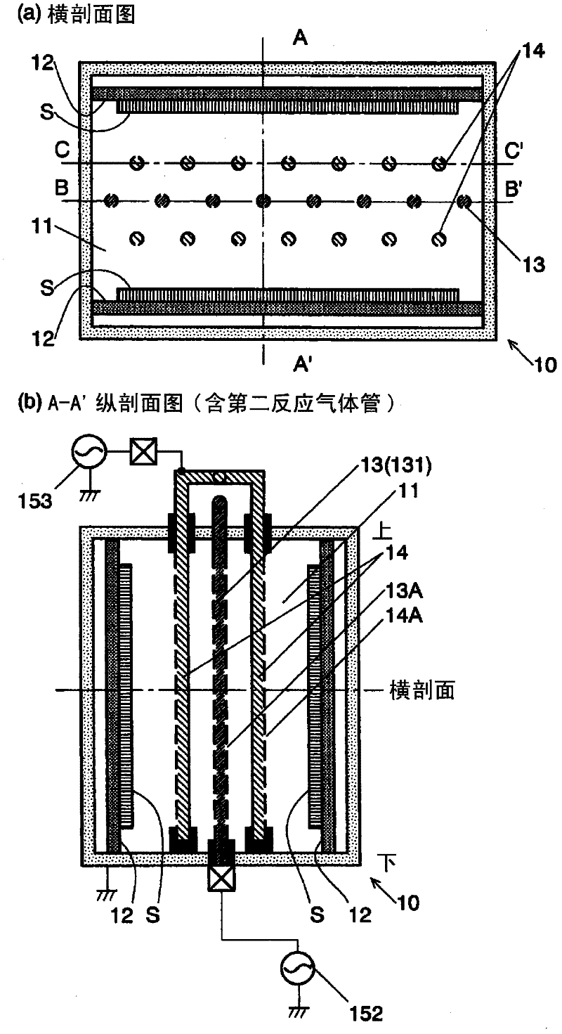
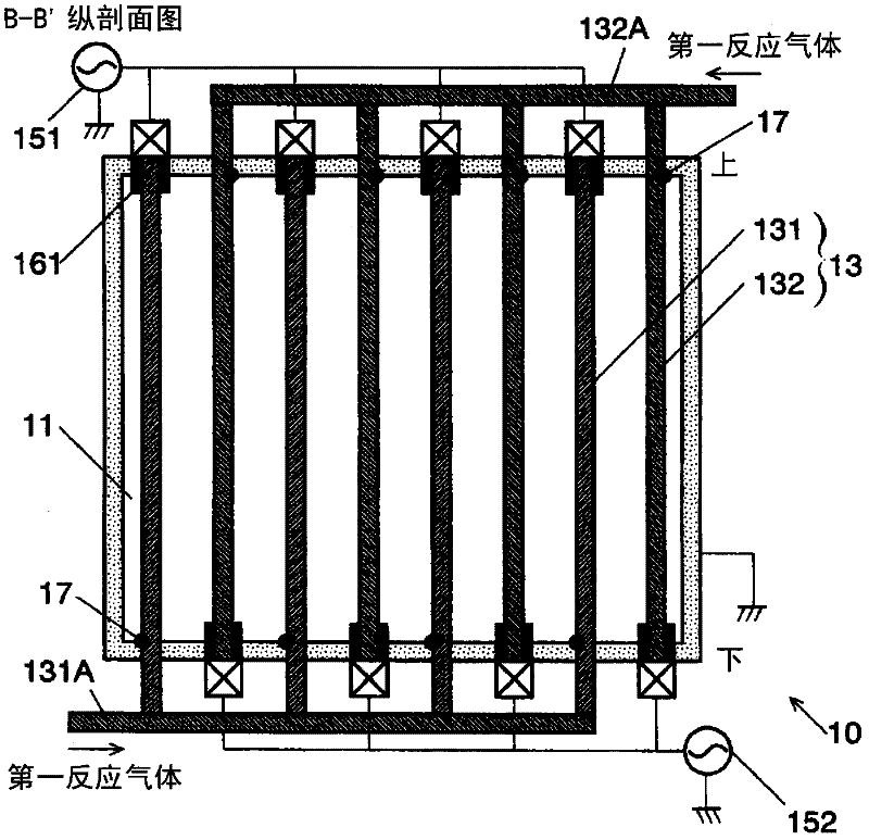
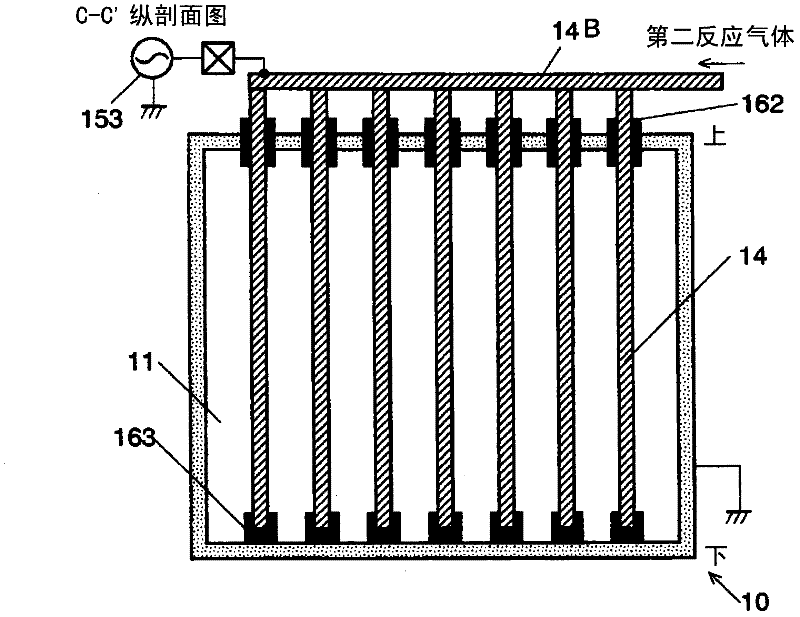
[0057] Figure 1 ~ Figure 3 shows the plasma processing apparatus 10 of the first embodiment, wherein figure 1 (a) is a cross-sectional view, figure 1 (b), figure 2 and image 3 Indicates longitudinal sections at mutually different positions.

[0058] The plasma processing apparatus 10 has the following: a plasma processing chamber 11 composed of a vacuum container; a pair of substrate holding parts 12 erected in a face-to-face manner in the plasma processing chamber 11; a plurality of first reaction gas pipes 13; a plurality of second reaction gas pipes 14 provided between each of the two substrate holding parts 12 and the first reaction gas pipes 13.

[0059] The substrate holder 12 is grounded via the wall surface of the plasma processing chamber 11 . In addition, a heater for heating the held substrate S is incorporated in the substrate holding portion 12 .

[0060] The first reactive gas pipe 13 is a pipe for supplying a first reactive gas into the plasma process...

Embodiment 2

[0073] use Figure 4 , to illustrate the second embodiment of the plasma processing apparatus of the present invention. In the plasma processing apparatus 10A of the second embodiment, one substrate holding portion 12A for substantially horizontally holding the substrate S is provided in the plasma processing chamber 11 . The substrate S is placed on the substrate holding portion 12A. Only one set of the second reaction gas tubes (electrodes) 14 is provided so as to match the number of the substrate holding parts 12A. In addition, a DC bias power supply 154 is connected to the second reaction gas pipe 14 . Except for these points, the plasma processing apparatus 10A of the second embodiment has the same configuration as the plasma processing apparatus 10 of the first embodiment. In addition, the operation of the plasma processing apparatus 10A of the second embodiment is also the same as that of the plasma processing apparatus 10 of the first embodiment.

Embodiment 3

[0075] use Figure 5 , a third embodiment of the plasma processing apparatus of the present invention will be described. In the plasma processing apparatus of the third embodiment, the high-frequency antenna 21 and the first reaction gas pipe 22 are provided independently. Specifically, the high-frequency antenna 21 is formed of linear conductor rods extending in the vertical direction, and is arranged in parallel in the plasma processing chamber 11 . To the high-frequency antenna 21, the first high-frequency power supply 151 or the second high-frequency power supply 152 is connected alternately in the order of arrangement so that currents flow in opposite directions. The first reaction gas pipes 22 are respectively provided on the upper wall and the lower wall of the plasma processing chamber 11 , and their open ends are arranged in the plasma processing chamber 11 . The first reaction gas pipe 22 is disposed between two adjacent high-frequency antennas. By arranging the r...


PUM


Abstract

A plasma processing apparatus (10) including: a plasma processing chamber (11) formed by a vacuum container; a pair of substrate holding units (12) arranged to face each other in the plasma processing chamber (11); a plurality of first reactive gas pipes (13) arranged between the two substrate holding units (12); and a plurality of second reactive gas pipes (14) arranged between the two substrate holding units (12) and the first reactive gas pipes (13). The first reactive gas pipes (13) are conductors which are connected to high-frequency power sources (151, 152). The second reactive gas pipes (14) are conductors which are electrically connected via a rectifier to an AC bias power source (153). The first reactive gas pipes (13) also serve as high-frequency antennas while the second reactive gas pipes (14) also serve as electrodes.

Description

technical field [0001] The present invention relates to a plasma processing apparatus that generates plasma and deposits on a planar substrate to be processed using the plasma. Background technique [0002] Plasma processing equipment is widely used to manufacture solar cells, displays, and the like. For example, when producing silicon thin-film solar cells, amorphous and crystalline silicon thin films are produced by plasma processing equipment. Among them, the photoelectric conversion wavelength range of the amorphous silicon thin film is on the shorter wavelength side than that of the crystalline silicon thin film, so it has the advantage of being able to increase the output power. On the other hand, a crystalline silicon thin film has a property that it is less likely to deteriorate than an amorphous silicon thin film. Among the crystalline silicon thin films, the silicon thin film composed of microcrystals has a photoelectric conversion wavelength range that is slight...

Claims


Application Information

Patent Timeline
IPC IPC(8): H01L21/205C23C16/509H01L31/04
CPCH01J37/3244C23C16/45578C23C16/509H01J37/32568
Inventor 井野英二渡边亮石原俊一芦田肇庄子博吉村桂一
Owner EBATEKKU
Why Eureka
Try Eureka