Schottky diode controlled by junction barrier having superposed P<+>-P structure

A technology of Schottky diode and junction barrier, which is applied in the direction of electrical components, circuits, semiconductor devices, etc., can solve the problems that Schottky contacts are easily affected by surface charges, large reverse leakage current, and high design requirements, and achieve reduction The effect of small number of carrier charges, improved reverse withstand voltage, and strong implementability

Inactive Publication Date: 2011-10-05
HARBIN ENG UNIV
View PDF4 Cites 7 Cited by
  • Summary
  • Abstract
  • Description
  • Claims
  • Application Information

AI Technical Summary

Problems solved by technology

[0005] JBS combines the advantages of both PiN and SBD to make it widely used, but compared with PiN diodes, JBS devices have larger reverse leakage current and lower reverse withstand voltage.
At the same time, ordinary junction barrier Schottky diodes have high requirements for junction terminal design, and Schottky contacts are easily affected by surface charges.

Method used


Image

  • Schottky diode controlled by junction barrier having superposed P&lt;+&gt;-P structure
  • Schottky diode controlled by junction barrier having superposed P&lt;+&gt;-P structure
  • Schottky diode controlled by junction barrier having superposed P&lt;+&gt;-P structure

Examples


Embodiment Construction

[0016] The present invention is described in more detail below in conjunction with accompanying drawing example:

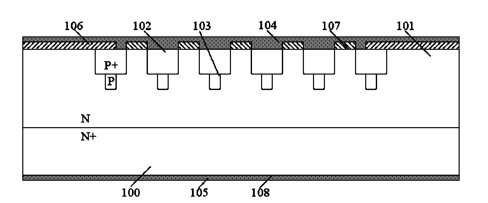
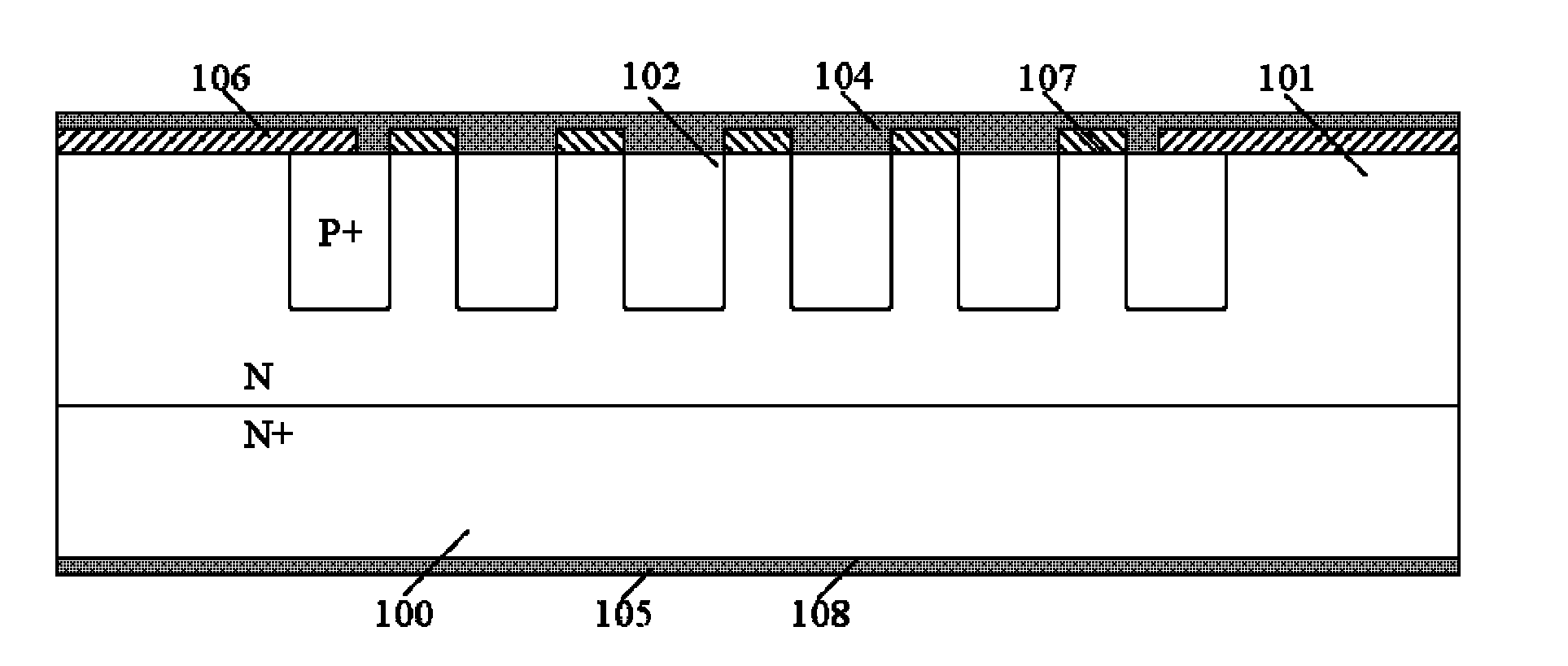
[0017] refer to figure 1 , the stacked P+-P junction barrier of the present invention controls the Schottky diode. Including N+ substrate region 100, N-type drift region 101, stacked P+-P structure P+ part 102, stacked P+-P structure P part 103, anode electrode 104, cathode electrode 105, silicon dioxide layer 106, Schottky Contact 107, ohmic contact 108. According to the requirements of the specific conduction characteristics and breakdown characteristics of the device, determine figure 1 The doping concentration and two-dimensional size of the drift region 101, and the two-dimensional size of the silicon dioxide layer 106.

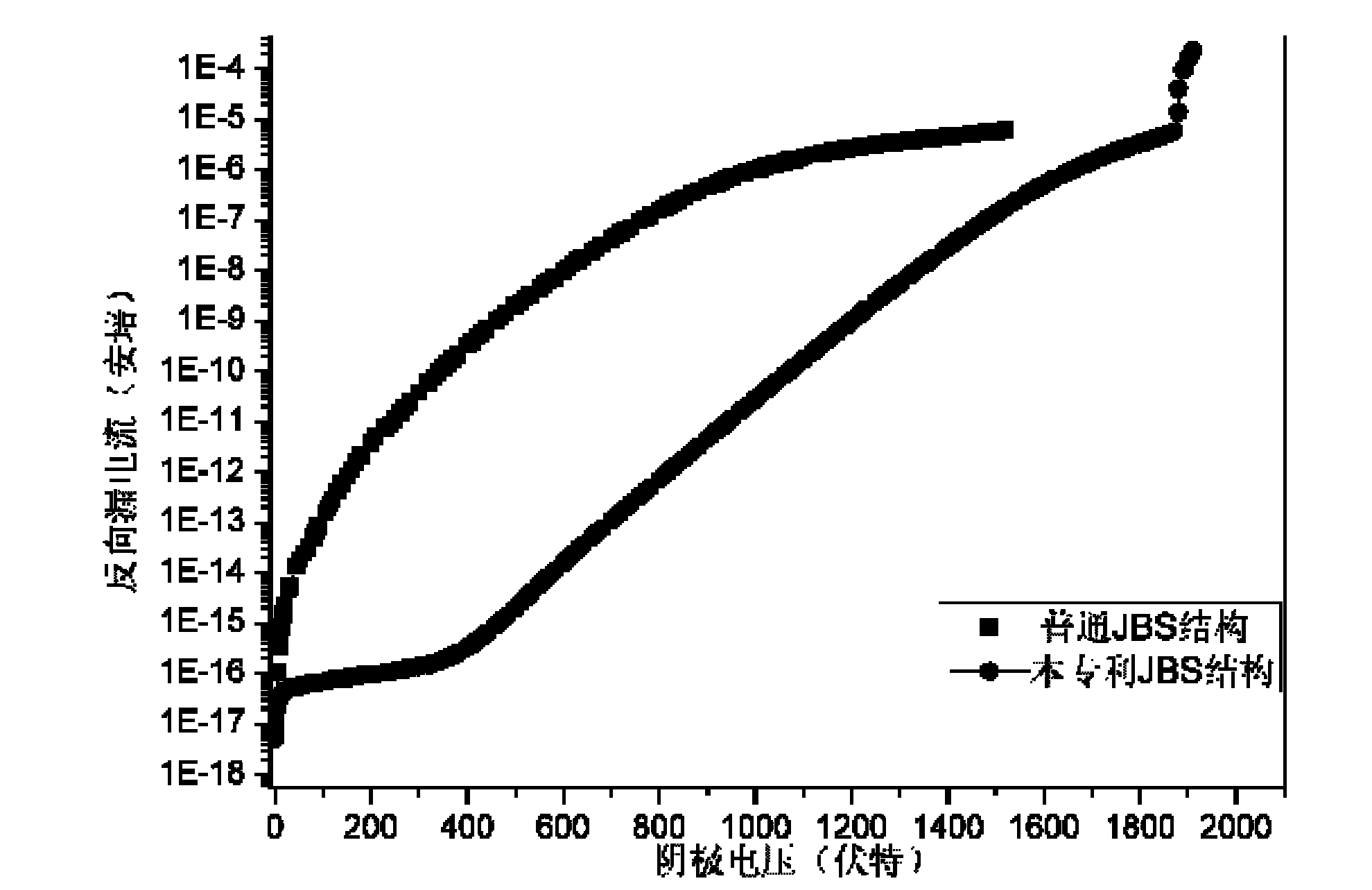
[0018] refer to image 3 , it can be seen from the comparison of the breakdown voltage characteristics of the stacked P+-P junction barrier controlled Schottky diode device of the present invention and the common junction barrier Schottk...


PUM


Abstract

The invention provides a schottky diode controlled by a junction barrier having a superposed P<+>-P structure. The schottky diode comprises an N<+> type substrate zone (100), an N type drift region (101), P<+> portions of the superposed P<+>-P structure (102), an anodic electrode (104), a cathodic electrode (105), a silicon dioxide layer (106), a schottky contact (107), and an ohmic contact (108). Besides, the schottky diode also includes P portions of the superposed P<+>-P structure (103), wherein the P<+> window portions of the superposed P<+>-P structure (102) is on the P window portions of the superposed P<+>-P structure (103). According to the invention, before the P<+> portions of the superposed P<+>-P structure in an area are formed, the P portions of the superposed P<+>-P structure in an area are formed, wherein the P portions are separated from each other and the structure of P portions is similar to the netted structure of a junction barrier schottky (JBS). Therefore, reverse withstand voltage of the JBS diode device can be improved and the output capacitance can be reduced, on the condition that the forward conduction characteristic of the device is not sacrificed. The process of the invention has the strong feasibility of implementation, and the application requirement of the power electronic system can be satisfied easily according to the invention.

Description

technical field [0001] The invention relates to an electronic device, specifically a Schottky diode. Background technique [0002] In the power system, a good rectifier requires small turn-on voltage, large turn-on current, low leakage current, high breakdown voltage and high switching speed, and having these characteristics at the same time is the ideal goal we pursue. In order to save energy, protect the environment, etc., we must reduce the power consumption of power devices as much as possible. [0003] A junction barrier Schottky diode (JBS) is a device that integrates a mesh PN junction in the drift region of the Schottky diode. The design of the mesh junction prevents the depletion region of the PN junction from being connected in the forward direction and zero bias. Therefore, in the forward direction, there are multiple conductive channels under the Schottky barrier for current to flow, and the device is turned on. . When a forward bias is applied to the N+ subst...

Claims


Application Information

Patent Timeline
Patent Type & Authority Applications(China)
IPC IPC(8): H01L29/872H01L29/06
CPCH01L29/872
Inventor 王颖李婷曹菲邵雷刘云涛
Owner HARBIN ENG UNIV
Why Eureka
Try Eureka