Silk solution, organic thin film transistor prepared by using silk solution, capacitor and manufacturing method thereof

An organic thin film and transistor technology, which is applied in the field of silk solution, organic thin film transistors and capacitors prepared by using the same, and a manufacturing method thereof, can solve the problems of increasing manufacturing cost and process complexity, and is beneficial to large-area production and improving transistors. Features, cheap effects

Inactive Publication Date: 2011-10-05
NATIONAL TSING HUA UNIVERSITY
View PDF3 Cites 7 Cited by
  • Summary
  • Abstract
  • Description
  • Claims
  • Application Information

AI Technical Summary

Problems solved by technology

[0010] In addition, whether it is an organic thin film transistor or a MIM capacitor structure, if a commonly used dielectric material is used, it is necessary to form a gate dielectric layer or an insulating layer through sputtering or vacuum deposition equipment, which often greatly increases the production cost and Process complexity

Method used


Image

  • Silk solution, organic thin film transistor prepared by using silk solution, capacitor and manufacturing method thereof
  • Silk solution, organic thin film transistor prepared by using silk solution, capacitor and manufacturing method thereof
  • Silk solution, organic thin film transistor prepared by using silk solution, capacitor and manufacturing method thereof

Examples


Embodiment 1

[0044] Example 1 - Top Contact Organic Thin Film Transistor Device

[0045] Preparation of silk aqueous solution

[0046] Firstly, prepare an aqueous solution containing 10 wt% sodium carbonate, heat it to boiling, add dry cocoons (natural silk) and boil for 30 minutes to 1 hour to remove sericin (sericin) on the outer layer of silk. Then, put it into deionized water for washing to wash away the lye attached to the outer layer of silk. After drying, the refined silk protein, namely fibroin, can be obtained.

[0047] Then, put the refined silk protein into 20ml of 85wt% phosphoric acid (H 3 PO 4 ) solution, stirred until dissolved. Then, the phosphoric acid solution dissolved in silk protein was put into a dialysis membrane (Spectra / Por 3 dialysis membrane, molecular weight cutoff = 14000) and dialyzed against water for 3 days to remove excess phosphate groups. By changing the volume of water used for dialysis and the number of dialysis times, in addition to removing phosp...

Embodiment 2

[0065] Example 2 - Bottom Contact Organic Thin Film Transistor Device

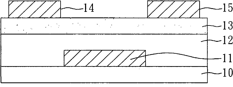
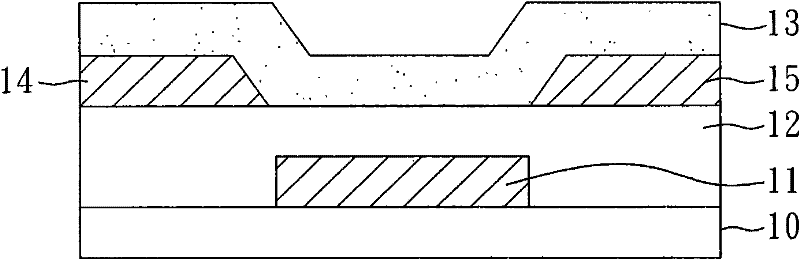
[0066] Such as Figure 6A As shown, a substrate 30 is provided, and a gate 31 and a gate dielectric layer 32 are sequentially formed on the substrate 30 . In this embodiment, the materials and preparation methods of the substrate 30 , the gate 31 , and the gate dielectric layer 32 are the same as those in the first embodiment. In addition, in this embodiment, the thickness of the gate 31 is about 100 nm, and the thickness of the gate dielectric layer 32 is about 500 nm.

[0067] Next, if Figure 6B As shown, a patterned metal layer is evaporated on the gate dielectric layer 32 to serve as the source 34 and the drain 35 by using the same process conditions as in the embodiment 1 for forming the gate. In this embodiment, the material of the source electrode 34 and the drain electrode 35 is gold, and its thickness is about 100 nm.

[0068] Finally, if Figure 6C As shown, an organic semiconductor layer 3...

Embodiment 3-MI

[0070] Embodiment 3-MIM capacitor structure

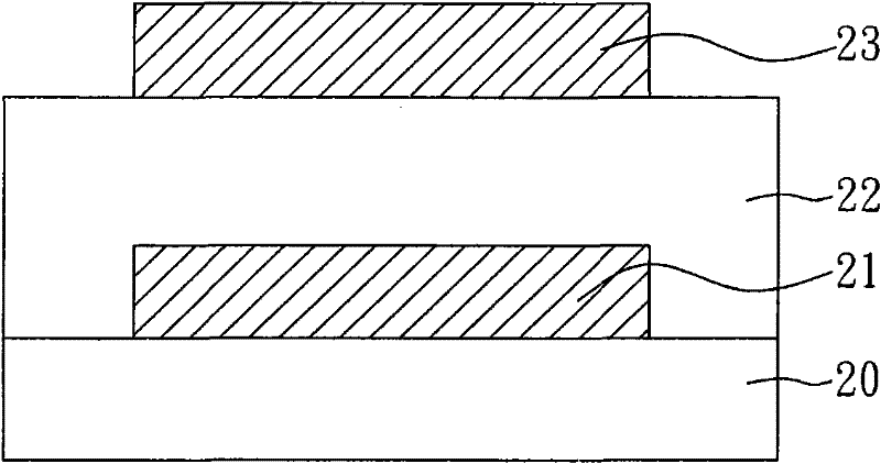
[0071] Such as Figure 7A As shown, a substrate 70 is provided, and a first electrode 71 is formed on the substrate 70 . In this embodiment, the manufacturing method of the first electrode 71 is the same as the gate manufacturing method described in the first embodiment. In this embodiment, the substrate 70 is a plastic substrate, and the material of the first electrode 71 is gold, and the thickness of the first electrode 71 is about 80 nm.

[0072] Then, the substrate 70 formed with the first electrodes 71 was immersed in the silk aqueous solution prepared in Example 1 for 15 minutes, so that the silk aqueous solution was coated on the substrate 70 formed with the first electrodes 71 . Then, drying the silk aqueous solution coated on the substrate 70 at 60° C. can form a silk film as an insulating layer 72, such as Figure 7B shown.

[0073] Finally, in a vacuum of 5×10 -6 The vacuum chamber (not shown) of torr is evaporated, t...


PUM


Abstract

The invention discloses silk solution, an organic thin film transistor prepared by using the silk solution, a capacitor and a manufacturing method thereof. The organic thin film transistor device comprises a substrate, a grid, a grid dielectric layer, an organic semiconductor layer, a source and a drain, wherein the grid is deployed on the substrate; the grid dielectric layer is deployed on the substrate and covers the grid, and the material of the grid dielectric layer contains a silk protein; and the organic semiconductor layer, the source and the drain are deployed above the grid dielectric layer.

Description

technical field [0001] The invention relates to a silk solution for electronic devices, an organic thin film transistor device with a silk protein dielectric layer prepared by using it, a metal-insulating layer-metal capacitor structure and a manufacturing method thereof, especially a kind of silk solution prepared by an aqueous solution process Silk solution for electronic devices, an organic thin film transistor device with a silk protein dielectric layer prepared by using it, a metal-insulating layer-metal capacitor structure and a manufacturing method thereof. Background technique [0002] In recent years, thin film transistors (TFTs) have been widely used in sensors, electronic tags (RFID) and display devices. In order to reduce the production cost of the product and expand the application range of the product, an organic thin film transistor (OTFT) that is low-cost, flexible, and can be produced in a large area is a research and development trend. [0003] In general,...

Claims


Application Information

Patent Timeline
Patent Type & Authority Applications(China)
IPC IPC(8): H01L51/05H01L51/30H01L51/40
Inventor 黄振昌王中桦谢兆莹
Owner NATIONAL TSING HUA UNIVERSITY
Why Eureka
Try Eureka