Semiconductor nanoparticle-based light emitting devices and associated materials and methods

A technology of nano-particles and light-emitting devices, which is applied in the direction of light-emitting materials, semiconductor devices, chemical instruments and methods, etc., can solve the problems of quantum yield decline, reduce the optical performance of quantum dots, photooxidation, etc., and achieve the effect of eliminating obstacles

Active Publication Date: 2011-10-12
NANOCO TECH LTD
View PDF13 Cites 36 Cited by
  • Summary
  • Abstract
  • Description
  • Claims
  • Application Information

AI Technical Summary

Problems solved by technology

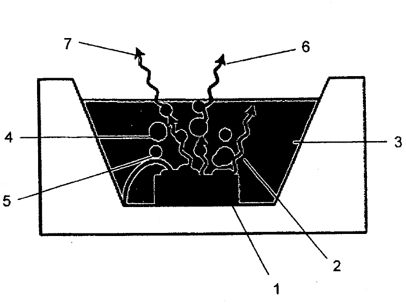
When incorporated into current LED encapsulation materials, quantum dots can agglomerate, degrading the optical properties of quantum dots
And once the quantum dots are added to the LED encapsulation material, oxygen may move through the encapsulation material to the surface of the quantum dots, which will cause photo-induced oxidation, and as a result, t...

Method used


Image

  • Semiconductor nanoparticle-based light emitting devices and associated materials and methods
  • Semiconductor nanoparticle-based light emitting devices and associated materials and methods
  • Semiconductor nanoparticle-based light emitting devices and associated materials and methods

Examples


example 1

[0102] Inclusion of quantum dots into suspended polymer beads

[0103] A 1% wt / vol solution of polyvinyl acetate (PVA) (aq) was prepared by stirring for 12 hours followed by extensive degassing by bubbling nitrogen through the solution for a minimum of 1 hour. Monomers, methyl methacrylate and ethylene glycol dimethacrylate were also degassed by nitrogen bubbling and used without further purification. Initiator AlBN (0.012 g) was placed in the reaction vessel and placed under three vacuum / nitrogen cycles to ensure the absence of oxygen.

[0104] The CdSe / ZnS core / shell quantum dots prepared as in Method 1 above were added into the reaction vessel in the form of a toluene solution, and the solvent was removed under reduced pressure. Degassed methyl methacrylate (0.98ml) was then added followed by degassed ethylene glycol dimethacrylate (0.15ml). The mixture was then stirred at 800 rpm for 15 minutes to ensure complete dispersion of the quantum dots within the monomer mixture....

example 2

[0110] Adsorption of quantum dots into prefabricated beads

[0111] Polystyrene microspheres with 1% divinylbenzene (DVB) and 1% thiol co-monomer were suspended in toluene (1 ml) by shaking and sonication. The microspheres were centrifuged (6000 rpm, about 1 minute), and the supernatant liquid was decanted. Washing again with toluene was repeated, and the pellet was suspended in toluene (1 ml).

[0112] InP / ZnS quantum dots prepared as described above in Method 2 were dissolved (excess, typically 5 mg for 50 mg of microspheres) in chloroform (0.5 ml) and filtered to remove any insoluble material. The quantum dot chloroform solution was added to the microspheres in toluene and shaken on a shaking plate at room temperature for 16 hours to mix thoroughly.

[0113] The quantum dot microspheres are centrifuged to form pellets, and the supernatant, which contains any quantum dots present in excess, is decanted. The pellet was washed twice with toluene (2ml) (as above), suspended ...

example 3

[0117] Inverse emulsion synthesis to form quantum dot-embedded silica beads

[0118] The InP / ZnS core / shell quantum dot solution (containing 70 mg of inorganic material) was evaporated to remove most of the quantum dot solvent, which in this example was toluene, and then mixed with a silane monomer (for example, 0.1 ml of 3-( Trimethoxysilyl)propyl methacrylate (TMOPMA) and 0.5 ml of tetramethoxysilane (TEOS)) were mixed until a clear solution was obtained.

[0119] Prepare 10 ml of degassed cyclohexane / Igepal in a 50 ml flask TM CO-520 (CO-520 is C 9 h 19 -Ph-(OCH 2 CH 2 )n-OH where n=5) (18ml / 1.35g), and inject 0.1ml of 4% NH 4 OH to form a stable inverse emulsion.

[0120] Then inject the quantum dots / silane mixture into cyclohexane / CO-520 / NH 4 in the OH mixture. at a rate of 500rpm at N 2 The resulting mixture was stirred overnight. Silica beads containing QDs were collected by centrifugation and washed twice with cyclohexane. The resulting precipitate was then...


PUM


Abstract

The present invention relates to a formulation for use in the fabrication of a light emitting device said formulation comprising a population of semiconductor nanoparticles incorporated into a plurality of discrete microbeads comprised of an optically transparent medium, said nanoparticle-containing medium being embedded in a host light emitting diode encapsulation medium. A method of preparing such a formulation is described. There is further provided a light emitting device including a primary light source in optical communication with such a formulation and a method of fabricating the same.

Description

technical field [0001] The present invention relates to semiconductor nanoparticle based light emitting devices and related materials and methods. In particular but not exclusively, the present invention relates to formulations for use in the fabrication of quantum dot-based light emitting devices and methods of producing such devices using said formulations. Background technique [0002] Light-emitting diodes (LEDs) are becoming increasingly important to modern day-to-day life, and they are expected to be used in many forms of lighting such as automotive lights, traffic lights, general lighting, liquid crystal display (LCD) backlights, and display screens. become one of the most important applications. Currently, LED devices are fabricated from inorganic solid-state compound semiconductors such as AlGaAs (red), AlGaInP (orange-yellow-green), and AlGaInN (green-blue), however, white-emitting solid-state LEDs cannot be produced using the mixture of available solid-state comp...

Claims


Application Information

Patent Timeline
IPC IPC(8): H01L33/50G01N33/53G01N33/58C09K11/00
CPCB82Y15/00C09K11/02C09K11/565C09K11/70C09K11/883G01N33/588H01L33/501H01L2924/181H01L2224/48091H01L33/502H01L2924/00012H01L2924/00014C09K11/00G01N33/53H01L33/50H01L33/505H01L33/52H01L33/005H01L33/56H01L2933/0041H01L2933/005H01L33/04
Inventor 奈杰尔·皮克特詹姆斯·哈里斯
Owner NANOCO TECH LTD
Why Eureka
Try Eureka