Method for preparing bunchy bismuth nanostructure material
A nanostructure and structural material technology, applied in the field of preparing bundled bismuth nanostructure materials, can solve the problems of inability to control a single size of a large area, inaccurate control of deposition time, low filling rate of filled nanowires, etc. Strong controllability and good periodicity
- Summary
- Abstract
- Description
- Claims
- Application Information
AI Technical Summary
Problems solved by technology
Method used
Image
Examples
Embodiment 1
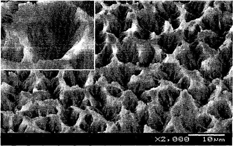
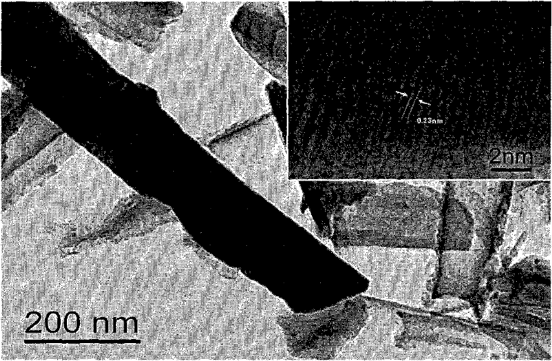
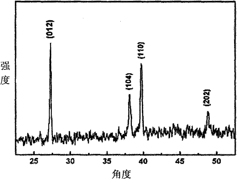
[0021] Preparation of bismuth beam nanostructure material, the specific steps are as follows:
[0022] a) Cut the alumina template into small pieces of 1cm×2cm, and then ultrasonically clean them in alcohol solution.
[0023] b) Prepare an electrodeposition solution consisting of 10 g / l BiCl 3 , 50g / l tartaric acid, 95g / l glycerol and 50g / l NaCl solution, the pH of the solution was adjusted to 0.9 with dilute hydrochloric acid.
[0024] c) Use CH1660C electrochemical workstation to conduct electrodeposition on alumina template, stage 1: at high level 1.5v, duration 0.4ms (milliseconds); low level 0v, duration 0.8ms (milliseconds), pulse under the above conditions Deposition for 40min (minutes). Stage 2: 2.5V DC electrodeposition for 1h (hour). Close the electrochemical deposition software to end the deposition.
[0025] d) After the electrodeposition is completed, the template is taken out, placed in deionized water, ultrasonically cleaned, then placed in NaOH (0.5 mol / l) ...
PUM
 Abstract
Description
Claims
Application Information


