Method for preparing photonic crystal slab waveguides

a technology of photonic crystal slab and waveguide, which is applied in the direction of microlithography exposure apparatus, photomechanical treatment, instruments, etc., can solve the problems of limiting the line width of waveguides, wasting time, and wasting electron beam or ion beam lithography time for defining waveguides in photonic crystals

Inactive Publication Date: 2009-08-06
NAT TAIWAN UNIV
View PDF5 Cites 5 Cited by
  • Summary
  • Abstract
  • Description
  • Claims
  • Application Information

AI Technical Summary

Benefits of technology

[0009]The object of the present invention is to provide a method for preparing photonic crystal slab waveguides, which combines Near-Field Phase-Shifting Contact Lithography (NFPSCL) and Interference Lithography (IL), to fabricate photonic crystal slab waveguides over a large area rapidly.

Problems solved by technology

However, either electron beam or ion beam lithography for defining the waveguides in photonic crystals is very time consuming because of inherent writing speed of each is too slow especially when the waveguides are long.
Furthermore, the waveguides can be defined rapidly in photonic crystals by the direct laser writing or the photolithography technique, but light diffraction may cause additional problems for waveguide patterning, limiting the line widths of waveguides.
Hence, it is difficult for the aforementioned methods to fabricate the photonic crystal slab waveguide over a large area composed of photonic crystal micro structures.

Method used


Image

  • Method for preparing photonic crystal slab waveguides
  • Method for preparing photonic crystal slab waveguides
  • Method for preparing photonic crystal slab waveguides

Examples


embodiment 1

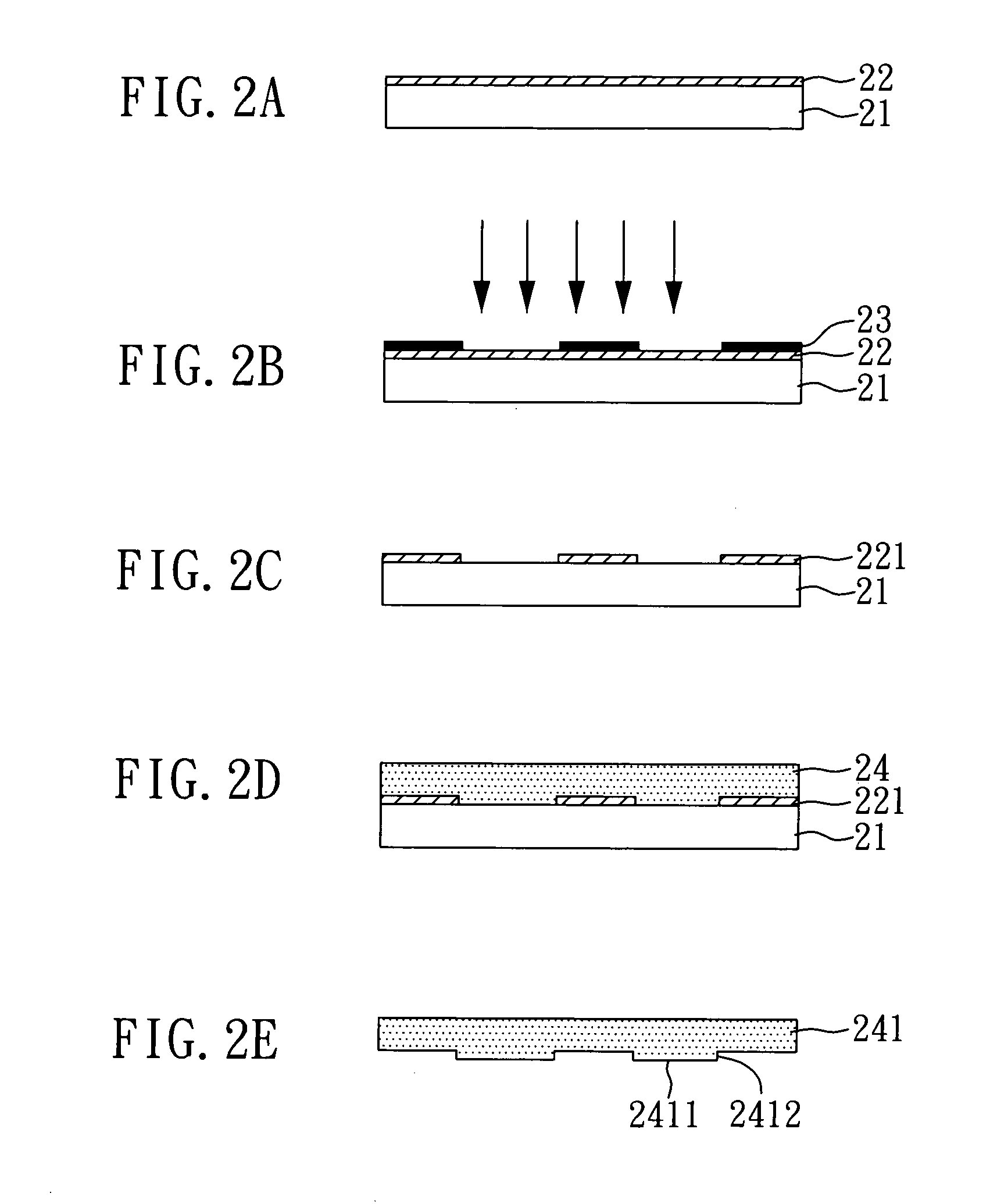
[0041]The method for preparing photonic crystal slab waveguides of the present embodiment is described with reference to FIG. 4A to FIG. 4H, wherein FIG. 4A to FIG. 4H are cross-sectional views showing a process for preparing a photonic crystal slab waveguides of the present embodiment.

[0042]The method for preparing photonic crystal slab waveguides of the present embodiment comprises the following steps:

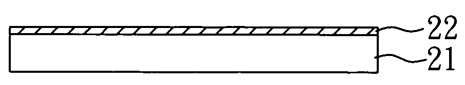
[0043]First, with reference to FIG. 4A, a substrate 41 is provided, wherein the material of the substrate 41 may be Si or SOI. In the present embodiment, the material of the substrate 41 is SOI.

[0044]A first metal layer 42 is deposited on the substrate 41 by e-gun evaporation (as shown in FIG. 4A), wherein the material of the first metal layer 42 may be Sn, Ag, Cu, Au, Cr, Ti, Zn, Ni, Cu—Cr alloy, Sn—Pb alloy. In the present embodiment, the material of the first metal layer 42 is Cr.

[0045]Then, a first photoresist layer 43 is coated on the first metal layer 42 by spinning coating, an...

embodiment 2

[0063]FIG. 6A to FIG. 6H are cross-sectional views showing a process for preparing a photonic crystal of the present embodiment.

[0064]First, with reference to FIG. 6A, a substrate 41 is provided. Then, a first metal layer 42, and a first photoresist layer 43 are disposed on the substrate 41. The first photoresist layer 43 is exposed and patterned by way of a phase-shift mask 44.

[0065]After removing the phase-shift mask 44, the first metal layer 42 is etched to form a waveguide pattern 421, as shown in FIG. 6B.

[0066]With reference to FIG. 6C, a second photoresist layer 46 is coated on the first metal layer 42 after the first photoresist layer 43 is removed.

[0067]With reference to FIG. 6D, plural first interference fringes are projected on the second photoresist layer 46 by coherent light beams. In the present embodiment, the line widths of each first interference fringes are the same, and the gaps between the adjacent first interference fringes are the same. Then, plural second inter...

embodiment 3

[0070]In methods for preparing photonic crystal slab waveguides disclosed in the embodiment 1 and embodiment 2, a photonic crystal pattern is formed after a waveguide pattern. However, in the present embodiment, the waveguide pattern is formed after the photonic crystal pattern.

[0071]FIG. 8A to FIG. 8C are cross-sectional views showing a process for preparing a photonic crystal of the present embodiment.

[0072]With reference to FIG. 8A, a first metal layer 42 and a second photoresist layer 46 are formed on the substrate 41 sequentially. Then, plural first interference fringes and plural second interference fringes are projected on the second photoresist layer 46 sequentially to pattern the second photoresist layer 46. Besides, the angles formed between the first interference fringes and the second interference fringes are 90°.

[0073]Plural third interference fringes may be formed on the second photoresist layer 46 by performing IL for the third time to pattern the second photoresist l...


PUM

PropertyMeasurementUnit
azimuth anglesaaaaaaaaaa
anglesaaaaaaaaaa
anglesaaaaaaaaaa

Abstract

A method for preparing a photonic crystal slab waveguides is disclosed, wherein the photonic crystal slab waveguides are prepared by combining near-field phase-shifting contact lithography (NFPSCL) with interference lithography (IL). Conventional methods used for preparing the photonic crystal slab waveguides, such as electron beam lithography or direct laser writing, are time consuming. In contrast, the present method allows rapid production of many photonic crystal slab waveguides over a large area composed of microstructures.

Description

BACKGROUND OF THE INVENTION[0001]1. Field of the Invention[0002]The present invention relates to a method for preparing photonic crystal slab waveguides and, more particularly, to a method for preparing photonic crystal slab waveguides for light transport.[0003]2. Description of Related Art[0004]Photonic crystals are composed of periodic dielectric structures, and the forms of the photonic crystals can be divided into 1-dimensional, 2-dimensional, and 3-dimensional structures. The photonic crystals can affect the light propagation through the periodic dielectric structures depending on the wavelength of the light. Besides, the photonic crystals are used in light transport, so the periodicity of photonic crystal structure has to be similar to the operating wavelength of light.[0005]Currently, progress in the semiconductor processing has enabled the photonic crystals to be realized. In addition, the photonic crystals can be applied widely in the fields of optical communication and opt...

Claims


Application Information

Patent Timeline
Patent Type & Authority Applications(United States)
IPC IPC(8): G03F7/20
CPCG03F1/14G03F1/34G03F1/26G03F1/50
Inventor WANG, LONLIN, MA KHINE ZARCHEN, YUNG-PIN
Owner NAT TAIWAN UNIV
Why Eureka
Try Eureka