Three-dimensional nano-structure array and preparation method and application thereof

A technology of three-dimensional nanometer and nanowire arrays, applied in nanotechnology, nanotechnology, nanotechnology for materials and surface science, etc., can solve the problems of high cost, sensitivity to light incident angle, low conversion rate of solar cells, etc., to achieve The effect of reducing preparation cost, reducing sensitivity, and increasing absorption area

Active Publication Date: 2017-07-25
SHANGQIU NORMAL UNIVERSITY
View PDF6 Cites 6 Cited by
  • Summary
  • Abstract
  • Description
  • Claims
  • Application Information

AI Technical Summary

Problems solved by technology

[0007] In order to solve the above problems, the object of the present invention is to provide a three-dimensional nanostructure array, a preparation method and its application. The application of the array in the field of photovoltaics can effectively solve the problems of low conversion rate of solar cells, sensitivity to light incident angle, and high cost.

Method used


Image

  • Three-dimensional nano-structure array and preparation method and application thereof
  • Three-dimensional nano-structure array and preparation method and application thereof

Examples


Embodiment 1

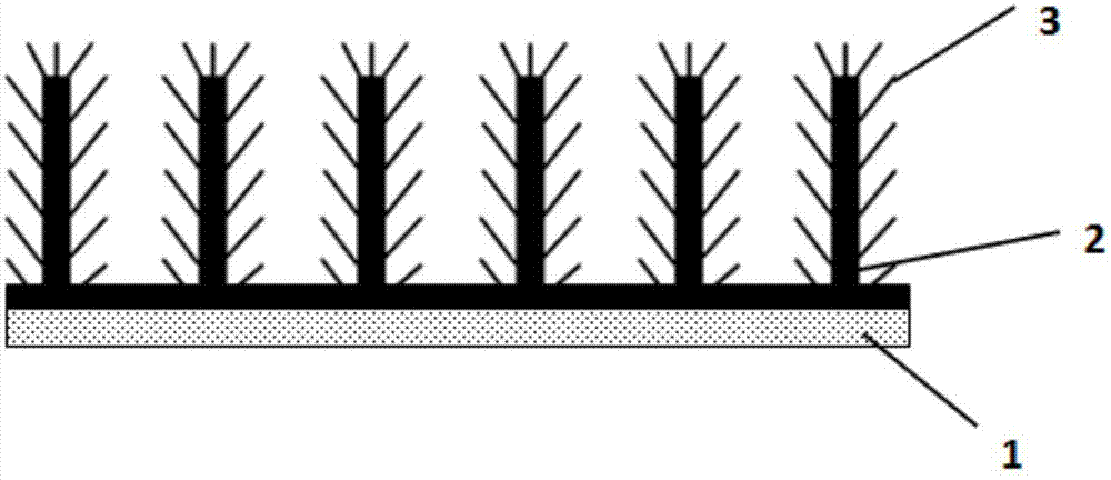
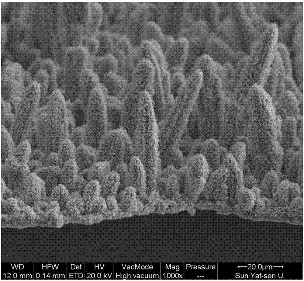
[0029] A kind of three-dimensional nanostructure array, its preparation method comprises the following steps:

[0030] (1) The glass sheet is ultrasonically cleaned with 1mol / L NaOH, 1mol / L HCl solution, absolute ethanol, and deionized water in sequence, and then a copper film is deposited on the glass sheet by a constant voltage electrochemical method, and the thickness of the copper film is 600nm ; Then put the substrate deposited with the copper film into the mixed gas of oxygen / hydrogen sulfide (volume ratio 1:2), react with gas and solid at 15°C for 20h, and the copper film is converted into a regularly arranged cuprous sulfide nanowire array;

[0031] (2) Copper particles are deposited on the surface of the cuprous sulfide nanowire array by the pulse voltage method; the size of the copper particles is 10nm;

[0032] (3) Put the cuprous sulfide nanowire array with copper particles deposited on the surface into the oxygen / hydrogen sulfide mixed gas (volume ratio 1:2), and ...

Embodiment 2

[0036] A kind of three-dimensional nanostructure array, its preparation method comprises the following steps:

[0037] (1) The glass sheet is ultrasonically cleaned with 1mol / L NaOH, 1mol / L HCl solution, absolute ethanol, and deionized water in sequence, and then a copper film is deposited on the glass sheet by a constant current electrochemical method, and the thickness of the copper film is 600nm ; Then put the substrate deposited with the copper film into the mixed gas of oxygen / hydrogen sulfide (volume ratio 1:2), react with gas-solid at 18°C ​​for 20h, and the copper film is converted into a regularly arranged cuprous sulfide nanowire array;

[0038] (2) Copper particles are deposited on the surface of the cuprous sulfide nanowire array by magnetron sputtering; the size of the copper particles is 15nm;

[0039] (3) Put the cuprous sulfide nanowire array with copper particles deposited on the surface into the oxygen / hydrogen sulfide mixed gas (volume ratio 1:2), and react ...

Embodiment 3

[0043] A kind of three-dimensional nanostructure array, its preparation method comprises the following steps:

[0044] (1) The glass sheet is ultrasonically cleaned with 1mol / L NaOH, 1mol / L HCl solution, absolute ethanol, and deionized water successively, and then a copper film is deposited on the glass sheet by a pulse current method, and the thickness of the copper film is 600nm; then Put the substrate deposited with the copper film into the oxygen / hydrogen sulfide mixed gas (volume ratio 1:2), and react with gas-solid at 25°C for 20h, and the copper film is converted into a regularly arranged array of cuprous sulfide nanowires;

[0045] (2) Copper particles are deposited on the surface of the cuprous sulfide nanowire array by magnetron sputtering; the size of the copper particles is 18nm;

[0046] (3) Put the cuprous sulfide nanowire array with copper particles deposited on the surface into the oxygen / hydrogen sulfide mixed gas (volume ratio 1:2), and react with gas-solid a...


PUM

PropertyMeasurementUnit
diameteraaaaaaaaaa
diameteraaaaaaaaaa
lengthaaaaaaaaaa

Abstract

The invention discloses a three-dimensional nano-structure array and a preparation method and an application thereof. The three-dimensional nano-structure array comprises regularly-arranged semiconductor nanowire arrays and semiconductor nanowire arrays grown in a radiation manner thereon. The nanowires grown in the prepared three-dimensional nano-structure array in a radiation manner are relatively small in diameters and relatively high in length and density, so that the specific surface area of the material is greatly enlarged, thereby enlarging the light absorption area of the three-dimensional nano-structure array and obviously reinforcing light absorption compared with a one-dimensional nanometer array; meanwhile, the fine and tiny nanowires are in radiation growth on the outer side of the regularly-arranged nanowires, and the nanowires grown in a radiation manner are relatively high in density, so that the light rays incident from each angle can be well absorbed, and sensitivity to the light ray incident angles of the three-dimensional nano-structure array is lowered; and when the three-dimensional nano-structure array is applied in the photovoltaic field, the problem of increasing of cost caused by a condition that the angle of a solar battery is changed constantly along with changes of illumination angles can be avoided.

Description

technical field [0001] The invention belongs to the technical field of solar photovoltaic cells, and in particular relates to a three-dimensional nanostructure array, a preparation method and an application thereof. Background technique [0002] With the development of nanotechnology and the improvement of people's requirements for photoelectric conversion efficiency, more and more researchers have begun to prepare nano-array solar cells, such as nano-rods, nano-wires, and nano-ribbon array solar cells. Among them, since the light absorption of nanowire solar cells occurs in the axial direction of the nanowires, the optical path is effectively increased and the absorption of light is increased; the separation of carriers occurs in the radial direction of the nanowires, which reduces the carrier density. The advantages such as the probability of recombination have received more attention. [0003] Chinese patent CN 102227002B discloses a polycrystalline silicon nanowire sola...

Claims


Application Information

Patent Timeline
Patent Type & Authority Applications(China)
IPC IPC(8): H01L31/032H01L31/0352H01L31/18B82Y30/00B82Y40/00
CPCB82Y30/00B82Y40/00H01L31/032H01L31/035227H01L31/18Y02P70/50
Inventor 李立强张文星丁艳丽王沙沙贾满满谷旭于佳卉
Owner SHANGQIU NORMAL UNIVERSITY
Why Eureka
Try Eureka