Method for improving electroplating quality of front electrode of solar cell
A technology of solar cells and front electrodes, which is applied in the field of solar cells, can solve problems affecting the appearance quality of cells, poor compactness of dielectric films, and decreased cell efficiency, so as to solve problems such as poor adhesion, good compactness, and reduced surface composite effect
- Summary
- Abstract
- Description
- Claims
- Application Information
AI Technical Summary
Problems solved by technology
Method used
Image

Examples
Embodiment 1
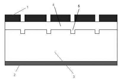
[0031] Such as figure 2 , image 3 As shown, the P-type silicon substrate 3 was cleaned and textured by the conventional process, and POCl was diffused at 850 °C 3 The liquid source was used for 25 minutes to obtain an N-type emitter 4 of about 50Ω / □. Edge isolation and PSG removal using wet chemical methods. After depositing a layer of SiNx film of about 90nm on the emitter by PECVD method as the dielectric film 1, screen-print aluminum paste and silver-aluminum paste on the side of the silicon substrate 3 without the dielectric film 1 as the back electric field 2 and the back electrode respectively, and then use The silver paste is screen-printed on the dielectric film 1 with a special screen plate with only the positive electrode of the busbar, and the width of the positive electrode of the busbar is 1.5 mm. The silicon substrate 3 that has completed the silk-screen printing process is passed into a sintering furnace for sintering at a temperature between 300°C and 900°...
Embodiment 2
[0033] Such as figure 2 , Figure 4 As shown, the P-type silicon substrate 3 is cleaned and textured by the conventional process, and then diffused with POCl at 830 °C 3 The liquid source was used for 25 minutes to obtain an N-type emitter 4 of about 100Ω / □. Edge isolation and PSG removal using wet chemical methods. After depositing a layer of SiNx film of about 90nm on the emitter by PECVD method as the dielectric film 1, screen-print aluminum paste and silver-aluminum paste on the side of the silicon substrate 3 without the dielectric film 1 as the back electric field 2 and the back electrode respectively, and then use The silver paste is screen-printed on the dielectric film 1 with a special screen plate with only the positive electrode of the busbar, and the width of the positive electrode of the busbar is 1.5 mm. The silicon substrate 3 that has completed the silk-screen printing process is passed into a sintering furnace for sintering at a temperature between 300°C a...
PUM
 Abstract
Description
Claims
Application Information
 - Generate Ideas
- Intellectual Property
- Life Sciences
- Materials
- Tech Scout
- Unparalleled Data Quality
- Higher Quality Content
- 60% Fewer Hallucinations
Browse by: Latest US Patents, China's latest patents, Technical Efficacy Thesaurus, Application Domain, Technology Topic, Popular Technical Reports.
© 2025 PatSnap. All rights reserved.Legal|Privacy policy|Modern Slavery Act Transparency Statement|Sitemap|About US| Contact US: help@patsnap.com