Array antenna used for reducing radar scattering cross section

A radar cross-section and array antenna technology, applied in the field of array antennas, can solve problems such as difficulties, increase in antenna volume, weight and cost, and enhance RCS, and achieve the effects of easy processing, simple structure, and stable shrinkage performance

Inactive Publication Date: 2011-10-26
XIDIAN UNIV
View PDF1 Cites 32 Cited by
  • Summary
  • Abstract
  • Description
  • Claims
  • Application Information

AI Technical Summary

Problems solved by technology

Try to hide the antenna when the radar is not working, and restore the antenna to the normal working state before the radar is turned on, so as to realize the stealth of the time-sharing antenna system. However, the stealth ability is completely lost when the radar is turned on
[0005] (2) Airspace Stealth
Since the theoretical basis of low-RCS stealth shape design is the geometrical optics approximation of high-frequency scattering, it is very effective in high-frequency bands, but in low-frequency bands, when the antenna size is similar to or even smaller than the radar operating wavelength, changing the shape has a great impact on RCS Small, it will even enhance RCS, and it will deteriorate the radiation performance of the antenna to a certain extent
For the stealth of out-of-band radar, there are many researches at present. F...

Method used


Image

  • Array antenna used for reducing radar scattering cross section
  • Array antenna used for reducing radar scattering cross section
  • Array antenna used for reducing radar scattering cross section

Examples


Embodiment 1

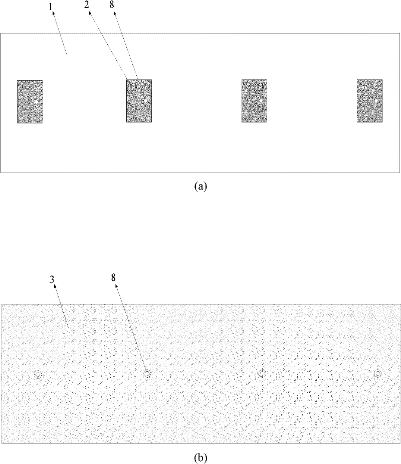
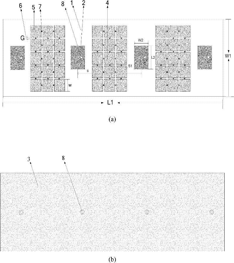
[0028] The length L1 of the dielectric plate 1 is 3λ, the width W1 is λ, the relative dielectric constant is 4.4, and the thickness is 0.06λ. The length L2 of the microstrip radiation unit 2 is 0.3λ, the width W2 is 0.2λ, the diameter D of the via hole 8 is 1.3 mm, and the center distance S of two adjacent microstrip radiation units is 0.8λ. The length and width W of the square metal patch 5 are both 0.14λ, and the width G of the gap 6 between adjacent metal patches 5 is 0.02λ. The distance S1 between the structured wave absorbing material array 4 and the adjacent side of the microstrip radiation unit 2 is 0.075λ, and the resistance value of the resistor 7 is 150 ohms. The number of the microstrip radiating unit 2 is n=4, the upper surface is a radiating surface, the lower surface is a grounding surface, and the upper and lower surfaces are connected by SMA heads. The capacitance C can be adjusted by changing the width G of the gap 6 between the metal patches 5, the inductance...

Embodiment 2

[0030] The length L1 of the dielectric plate 1 is 6λ, the width W1 is λ, the relative dielectric constant is 4.4, and the thickness is 0.03λ. The length L2 of the microstrip radiation unit 2 is 0.3λ, the width W2 is 0.2λ, the diameter D of the via hole 8 is 1.3 mm, and the center distance S between two adjacent microstrip radiation units is λ. This embodiment is a cross metal patch, and its length and width W are both 0.05λ, and the width G of the gap 6 between adjacent metal patches 5 is 0.06λ. The distance S1 between the structured wave absorbing material array 4 and the adjacent side of the microstrip radiation unit 2 is 0.32λ, and the resistance value of the resistor 7 is 500 ohms. The number of microstrip radiating units 2 is n=8, the upper surface is a radiating surface, the lower surface is a grounding surface, and the upper and lower surfaces are connected by SMA heads. The capacitance C can be adjusted by changing the width G of the gap 6 between the metal patches 5, ...

Embodiment 3

[0032] The length L1 of the dielectric plate 1 is 25λ, the width W1 is λ, the relative dielectric constant is 4.4, and the thickness is 0.02λ. The length L2 of the microstrip radiation unit 2 is 0.3λ, the width W2 is 0.2λ, the diameter D of the via hole 8 is 1.3 mm, and the center distance S of two adjacent microstrip radiation units is 2λ. This embodiment is a circular metal patch, the diameter W of which is 0.5λ, and the width G of the gap 6 between adjacent metal patches 5 is 0.01λ. The distance S1 between the structured wave-absorbing material array 4 and the adjacent side of the microstrip radiation unit 2 is 0.15λ, and the resistance value of the resistor 7 is 1 ohm. The number of microstrip radiating units 2 is n=128, the upper surface is a radiating surface, the lower surface is a grounding surface, and the upper and lower surfaces are connected by SMA heads. The capacitance C can be adjusted by changing the width G of the gap 6 between the metal patches 5, the inducta...


PUM

PropertyMeasurementUnit
Resistanceaaaaaaaaaa
Diameteraaaaaaaaaa
Resistanceaaaaaaaaaa

Abstract

The invention discloses an array antenna used for reducing radar scattering cross section, and mainly solves a problem of large scattering cross section of a present microstrip array antenna radar. The array antenna in the invention comprises a medium plate, a ground plate and n microstrip radiation units (2). The n microstrip radiation units (2) are on the upper surface of the medium plate (1). The ground plate (3) is on the lower surface of the medium plate (1). Structural type absorbing material arrays (4) are provided between each two adjacent microstrip radiation units, and N*M square metal pasters (5) are arranged as rectangular. The metal pasters (5) form inductances L. Connection resistors (7) connect adjacent metal pasters to form resistors R. Gap (6) between adjacent metal pasters (5) form capacitors C. The capacitors C, the inductances L and the resistors R form RLC resonance circuits. By adjusting resonance circuits frequency to superpose the resonance circuits frequency with antenna work frequency, absorption of vertical incident surface wave is realized. The array antenna used for reducing radar scattering cross section in the invention has the advantages of stable performance of reducing in-band and outband radar scattering cross sections of antenna and no influence on antenna volume, weight and cost.

Description

Technical field [0001] The invention belongs to the technical field of antennas, in particular to an array antenna that utilizes structural wave absorbing materials to reduce the radar cross section, and is used to realize antenna stealth. Background technique [0002] In various aircraft, the antenna is an indispensable component, and the problem of its radar cross section RCS contributing to the overall RCS of the aircraft has become more prominent. Due to the limitation of the working characteristics of the antenna system, it must ensure the normal reception and transmission of its own electromagnetic waves. Therefore, conventional stealth measures cannot simply be used in antenna stealth. How to reduce the RCS of the antenna so that the antenna system can work effectively without being detected and attacked by the other party not only affects the survival of the antenna itself, but also affects the electromagnetic stealth performance of its carrier, which in turn affects the ...

Claims


Application Information

Patent Timeline
IPC IPC(8): H01Q13/08H01Q1/38H01Q17/00H01Q21/00G01S7/02
Inventor 张鹏飞王夫蔚路宝龚琦徐云学龚书喜刘英姜文
Owner XIDIAN UNIV
Why Eureka
Try Eureka