

Method for preparing metal nano stripes
A metal nano and stripe technology, applied in the field of new materials, to achieve the effect of high efficiency, large-scale industrial production, and easy large-scale industrial production
- Summary
- Abstract
- Description
- Claims
- Application Information
AI Technical Summary
Problems solved by technology
Method used
Image

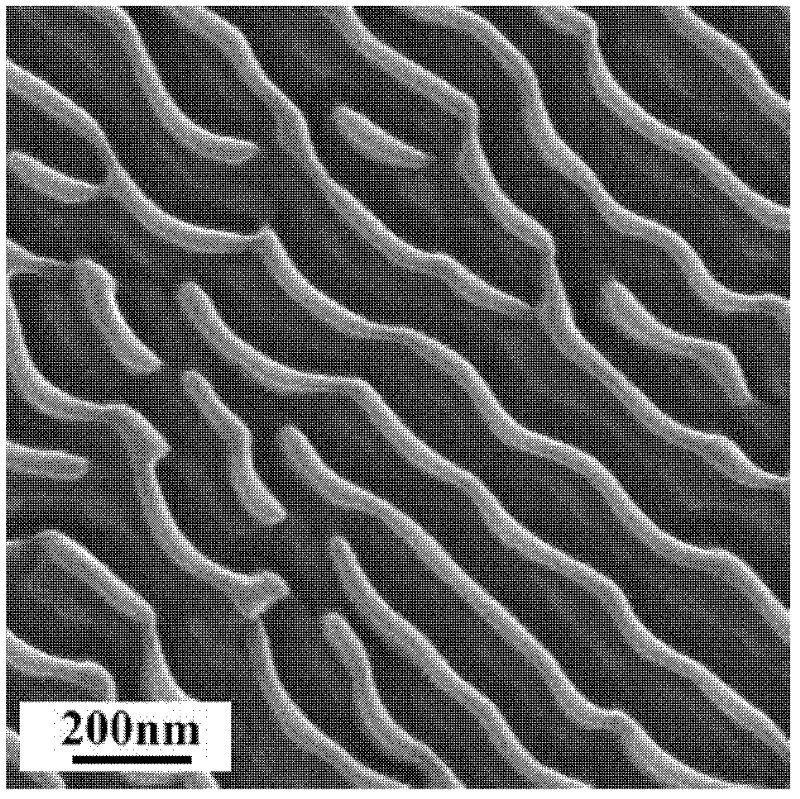
Examples
Embodiment 1
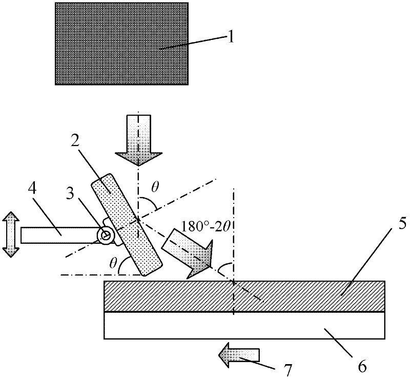
[0018] Kaufmann-type wide-beam ion source bombardment system is adopted, the ion beam spot diameter is 50 mm, high-purity Ar (99.999%) is used as the working gas, and the background vacuum is 2×10 -4 Pa, the working pressure is 2×10 -2 Pa. The substrate material is an EPI-polished N-type single crystal Si(100) substrate, the resistance of which is 0.01Ω·cm-0.02Ω·cm, and the surface roughness is 0.2nm. The substrate Si (100) substrate was ultrasonically cleaned with acetone, absolute ethanol, and deionized water for 15 minutes in advance to remove organic and inorganic impurities. Use a high-purity Fe (99.995%) block with a flat surface and a rectangular structure as the metal target, set the horizontal angle between the target surface and the substrate workbench to be 80°, and the bottom position of the target and the substrate Si (100) substrate The vertical height is 1mm. The working table temperature is normal temperature 25°C, and the horizontal movement speed is 0.05cm...
Embodiment 2
[0020] Kaufmann-type wide-beam ion source bombardment system is adopted, the ion beam spot diameter is 50 mm, high-purity Ar (99.999%) is used as the working gas, and the background vacuum is 2×10 -4 Pa, the working pressure is 2×10 -2Pa. The substrate material is an EPI-polished P-type single crystal Si(111) substrate, the resistance of which is 5.6Ω·cm-10.4Ω·cm, and the surface roughness is 0.2nm. The substrate Si(111) substrate was ultrasonically cleaned with acetone, absolute ethanol, and deionized water for 15 minutes in advance to remove organic and inorganic impurities. A high-purity Co (99.995%) block with a flat surface and a rectangular structure is used as a metal target, and the horizontal angle between the target surface and the substrate workbench is set at 55°, and the bottom position of the target and the substrate Si (111) substrate The vertical height is 1mm. The temperature of the workbench is maintained at 700°C, and the horizontal movement speed is 0.02...
PUM
| Property | Measurement | Unit |
|---|---|---|
| surface roughness | aaaaa | aaaaa |
| surface roughness | aaaaa | aaaaa |
Abstract
Description
Claims
Application Information