Diode chip and processing technology thereof

A processing technology and diode technology, applied in the direction of electrical components, electric solid devices, circuits, etc., can solve problems such as poor withstand voltage, chip creepage, easy discharge, etc., to improve diode withstand voltage and enhance device stability , Improve the effect of pressure resistance

Active Publication Date: 2011-11-16
扬州杰利半导体有限公司
View PDF5 Cites 7 Cited by
  • Summary
  • Abstract
  • Description
  • Claims
  • Application Information

AI Technical Summary

Problems solved by technology

If the test is carried out in the air, it is easy to generate discharge between the corners (90° angle), and even burn the chip
[0003] With the improvement of the application requirements of diodes in protection circuits, in order to solve the problems of tip discharge and poor withstand voltage conditions, the currently commonly used chip solutions are relatively simple: either there is no SIPOS passivation layer, and it is impossible to overcome the movable surface of the chip. The interference of ions can easily

Method used


Image

  • Diode chip and processing technology thereof
  • Diode chip and processing technology thereof
  • Diode chip and processing technology thereof

Examples


Embodiment Construction

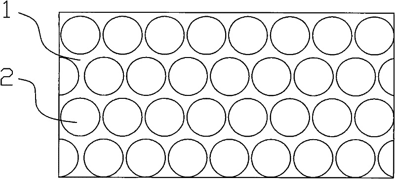
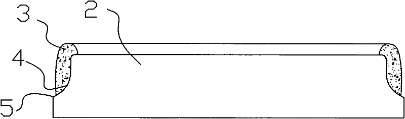
[0021] Diode chip of the present invention such as figure 1 , 2 As shown: the edge of the chip 2 is provided with a circle of glass protective layer 3, and the horizontal projection of the chip 2 is a closed shape without corners; the longitudinal section of the chip 2 is convex, and the upper part of the side is concave arc-shaped, The lower part is a straight side; the side is provided with a circle of semi-insulating polysilicon film (SIPOS film) 4; the glass protective layer 3 covers 70-95% of the upper part of the semi-insulating polysilicon film 4. An exposed section 5 is kept to prevent a gold layer from adhering to it when steaming gold.

[0022] Process of the present invention such as figure 1 , 2 Shown: Include the following steps:

[0023] 1), the engraving of wafer 1 split pattern; using a mask plate, and then processing grooves on the wafer by coating photoresist, soft baking, exposure, development, fixing and hard baking, so that the chips between the groo...


PUM


Abstract

The invention provides a diode chip and a processing technology thereof, relating to a semiconductor discrete device and a processing technology thereof. The invention can overcome discharge in detection and creepage phenomenon in use. A circle of glassy protective layer is arranged at the edge of a chip, the horizontal projection of the chip is of a closed shape with no corner; the side edge is provided with a circle of semi-insulating polycrystalline silicon (SIPOS) film; and the glassy protective layer covers 70-95% of the upper part of the SIPOS film. The processing technology provided bythe invention comprises the following steps: 1) graving a wafer split pattern; 2) passivating the SIPOS film; 3) processing the glassy protective layer; 4) photoengraving three times; 5) cleaning; 6)removing photoresist; 7) splitting to obtain the chip. By the adoption of the invention, the point discharge of a square chip can be effectively prevented and the withstand voltage capacity of a diode can be improved. Before passivation with glass, passivation with an SIPOS film is carried out to absorb movable ions on the surface of the chip, thus the stability can be enhanced and the withstand voltage capacity can be improved; meanwhile, the bottoms of grooves still remains the SIPOS film and an SIO2 film, thus preventing Au layer adhesion in Au evaporation.

Description

technical field [0001] The invention relates to a semiconductor discrete device and its processing technology, in particular to a diode chip integrating circular shape, SIPOS (semi-insulating polysilicon) passivation and PHOTO GLASS manufacturing process and its processing technology. Background technique [0002] At present, most of the products in the diode market are square for the convenience of splitting and processing, such as image 3 shown. If the test is carried out in the air, it is easy to generate discharge between the knuckles (90° angle), and even burn the chip. [0003] With the improvement of the application requirements of diodes in protection circuits, in order to solve the problems of tip discharge and poor withstand voltage conditions, the currently commonly used chip solutions are relatively simple: either there is no SIPOS passivation layer, and it is impossible to overcome the movable surface of the chip. The interference of ions can easily cause reve...

Claims


Application Information

Patent Timeline
IPC IPC(8): H01L23/29H01L21/316
Inventor 汪良恩裘立强魏兴政
Owner 扬州杰利半导体有限公司
Why Eureka
Try Eureka