

Controlled silicon chip structure of mesa technology and implementation method
A silicon chip and process technology, applied in the manufacture of transistors, electrical components, semiconductor/solid-state devices, etc., can solve the problems of high fragmentation rate of silicon wafers, generation of waste products, and difficulty, and achieve good breakdown voltage characteristics and reduce fragmentation. rate, glass expansion coefficient reduction effect
- Summary
- Abstract
- Description
- Claims
- Application Information
AI Technical Summary
Problems solved by technology
Method used
Image

Examples
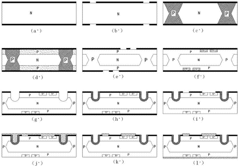
Embodiment 1
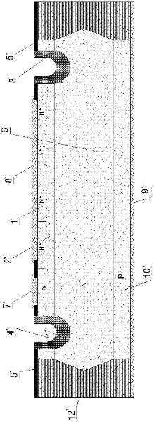
[0019] Such as Figure 5 As shown, the mesa process thyristor chip structure of the present invention includes N + Type cathode region 1, front P-type short base region 2, glass passivation film 3, front trench 4, SiO 2 Protective film 5, silicon single wafer 6, gate aluminum electrode 7 and cathode aluminum electrode 8, silicon single wafer 6 front is provided with front P-type short base region 2, silicon single wafer 6 back is provided with rear P-type area 10, front P The surface of the type short base region 2 is provided with SiO 2 The protective film 5, the gate aluminum electrode 7 and the cathode aluminum electrode 8, the front P-type short base region 2 and the silicon single wafer 6 are provided with a front groove 4, and the front groove 4 is located on the gate aluminum electrode 7 and the cathode aluminum electrode 8 On both sides, there is a N between the cathode aluminum electrode 8 and the front P-type short base region 2 + type cathode region 1, the back s...
Embodiment 2
[0035] Such as Figure 5 As shown, the mesa process thyristor chip structure of the present invention includes N + Type cathode region 1, front P-type short base region 2, glass passivation film 3, front trench 4, SiO 2 Protective film 5, silicon single wafer 6, gate aluminum electrode 7 and cathode aluminum electrode 8, silicon single wafer 6 front is provided with front P-type short base region 2, silicon single wafer 6 back is provided with rear P-type area 10, front P The surface of the type short base region 2 is provided with SiO 2 The protective film 5, the gate aluminum electrode 7 and the cathode aluminum electrode 8, the front P-type short base region 2 and the silicon single wafer 6 are provided with a front groove 4, and the front groove 4 is located on the gate aluminum electrode 7 and the cathode aluminum electrode 8 On both sides, there is a N between the cathode aluminum electrode 8 and the front P-type short base region 2 + type cathode region 1, the back s...
Embodiment 3
[0051] Such as Figure 5 As shown, the mesa process thyristor chip structure of the present invention includes N + Type cathode region 1, front P-type short base region 2, glass passivation film 3, front trench 4, SiO 2 Protective film 5, silicon single wafer 6, gate aluminum electrode 7 and cathode aluminum electrode 8, silicon single wafer 6 front is provided with front P-type short base region 2, silicon single wafer 6 back is provided with rear P-type area 10, front P The surface of the type short base region 2 is provided with SiO 2 The protective film 5, the gate aluminum electrode 7 and the cathode aluminum electrode 8, the front P-type short base region 2 and the silicon single wafer 6 are provided with a front groove 4, and the front groove 4 is located on the gate aluminum electrode 7 and the cathode aluminum electrode 8 On both sides, there is a N between the cathode aluminum electrode 8 and the front P-type short base region 2 + type cathode region 1, the back s...
PUM
| Property | Measurement | Unit |
|---|---|---|
| Depth | aaaaa | aaaaa |
| Width | aaaaa | aaaaa |
| Thickness | aaaaa | aaaaa |
Abstract
Description
Claims
Application Information