Silicon-based waveguide grating coupler on insulator and preparation method thereof

A silicon-on-insulator, waveguide grating technology, which is applied in the coupling of optical waveguides, light guides, optics, etc., can solve the problems of difficult on-line testing and packaging of devices, reduced process tolerances, and increased manufacturing costs. Process tolerance, effect of efficient coupling

Inactive Publication Date: 2011-11-23
ZHEJIANG ORIENT CRYSTAL OPTICS
View PDF4 Cites 24 Cited by
  • Summary
  • Abstract
  • Description
  • Claims
  • Application Information

AI Technical Summary

Problems solved by technology

However, as the size of the SOI optical waveguide shrinks, the mode spot size of the light in the waveguide also becomes smaller than 1 μm, while the mode spot size in the optical fiber is 8-10 μm. The matching will lead to the appearance of radiation mode and back reflection, and the light entering such a small-sized waveguide from the optical fiber will often cause a large loss, which brings great difficulties to the on-line test of the device and subsequent packaging. performance is also limited
Therefore, in the field of integrated optoelect

Method used


Image

  • Silicon-based waveguide grating coupler on insulator and preparation method thereof
  • Silicon-based waveguide grating coupler on insulator and preparation method thereof
  • Silicon-based waveguide grating coupler on insulator and preparation method thereof

Examples


Embodiment Construction

[0026] Below in conjunction with accompanying drawing and embodiment structure and feature of the present invention are described in further detail:

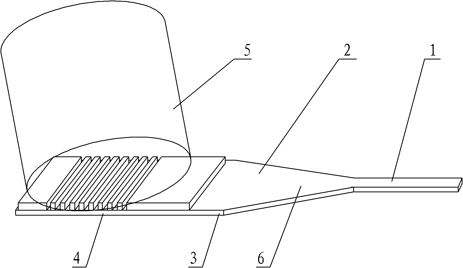
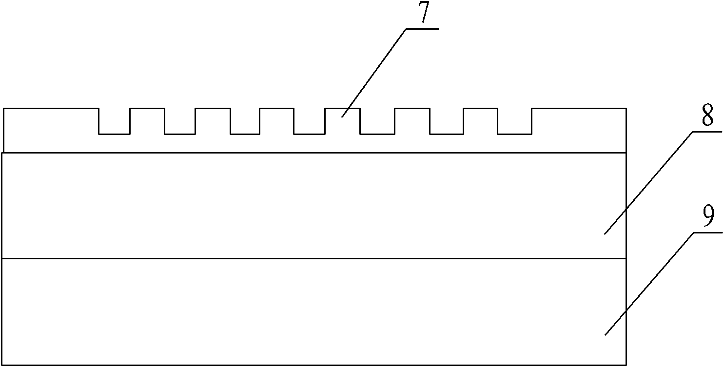
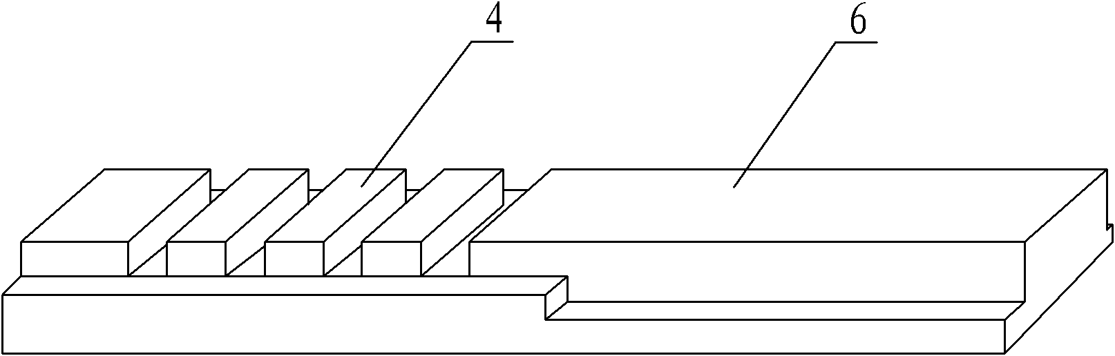
[0027] Such as figure 1 , figure 2 , image 3 As shown, a silicon-on-insulator-based waveguide grating coupler includes a silicon-on-insulator (SOI) sheet, which is characterized in that: the SOI sheet is composed of a silicon substrate 9, a confinement layer 8, and a top silicon layer 7, and the confinement layer 8 On the silicon substrate 9, the top silicon layer 7 is made on the confinement layer 8, a diffraction grating 4 is made on the surface of the top silicon layer 7, and on the other side of the diffraction grating 4 are a wide waveguide 3 and a tapered waveguide 2, the The length of the tapered waveguide 2 is greater than 100 μm, and the submicron waveguide 1 is connected with the tapered waveguide 2. There is an optical fiber 5 for receiving diffracted light above the diffraction grating on the top silicon layer, a...


PUM

PropertyMeasurementUnit
Thicknessaaaaaaaaaa
Thicknessaaaaaaaaaa
Areaaaaaaaaaaa

Abstract

The invention relates to photonic device technical field, concretely providing a silicon-based waveguide grating coupler on an insulator and a preparation method thereof. The grating coupler comprises a Silicon-On-Insulator (SOI) chip. The SOI chip is characterized in that: the SOI chip is composed of a silicon substrate, a restriction layer and a top silicon layer, wherein the restriction layer is above the silicon substrate, the top silicon layer is above the restriction layer, a surface of the top silicon layer is provided with diffraction grating, a broad waveguide, a taper waveguide and a submicron waveguide connecting with the taper waveguide are provided at an opposite side of the diffraction grating, and a fiber used for receiving diffracted light is provided above the diffraction grating on the top silicon layer. The invention provides a preparation method of the grating coupler, electron beam exposure and common lithography are combined, which means that fine grating and the submicron waveguide structure are defined by the high precision electron beam exposure and a second silicon etching window is defined by the low precision common lithography, thus technology tolerance of production is substantially raised and integrity of a fine structure is guaranteed.

Description

technical field [0001] The invention relates to the technical field of photonic devices, in particular to a silicon-on-insulator waveguide grating coupler and a preparation method thereof. Background technique [0002] Since the beginning of the new century, with the continuous development of micro-nano optoelectronic integration technology, the integration of chips has become higher and higher, the size of devices has been continuously reduced, and the waveguide used to transmit optical signals has gradually shrunk to the sub-micron scale. Among the many optical waveguide materials used in the communication band, silicon-on-insulator (SOI) materials are easy to produce submicron-level low-loss optical waveguides due to the strong light confinement ability of the waveguide layer; at the same time, the preparation process is compatible with the microelectronic IC process , which greatly reduces the cost of preparing optoelectronic chips, making it one of the most competitive ...

Claims


Application Information

Patent Timeline
IPC IPC(8): G02B6/34G02B6/124G02B6/136
Inventor 李京波李庆跃李凯董珊颜晓升池旭明李树深夏建白
Owner ZHEJIANG ORIENT CRYSTAL OPTICS
Why Eureka
Try Eureka