Controlled silicon device under auxiliary trigger of embedded P-type MOS (Metal Oxide Semiconductor) transistor

A technology of MOS tube and silicon device, applied in the field of thyristor device, can solve the problems of increasing the area of ​​thyristor device, limited clamping voltage, increasing cost, etc., to achieve economical and effective working voltage, increase clamping voltage, low working The effect of voltage

Inactive Publication Date: 2012-10-24
ZHEJIANG UNIV
View PDF2 Cites 0 Cited by
  • Summary
  • Abstract
  • Description
  • Claims
  • Application Information

AI Technical Summary

Problems solved by technology

However, a disadvantage of this method is that the improvement of the clamping voltage by increasing the base width of the parasitic transistor is very limited. The width of the base area of ​​the triode is stretched to a large distance, which greatly increases the area of ​​the thyristor device on the silicon wafer and increases the cost of device manufacturing

Method used


Image

  • Controlled silicon device under auxiliary trigger of embedded P-type MOS (Metal Oxide Semiconductor) transistor
  • Controlled silicon device under auxiliary trigger of embedded P-type MOS (Metal Oxide Semiconductor) transistor
  • Controlled silicon device under auxiliary trigger of embedded P-type MOS (Metal Oxide Semiconductor) transistor

Examples


Embodiment Construction

[0020] The present invention will be described in detail below in conjunction with the embodiments and accompanying drawings, but the present invention is not limited thereto.

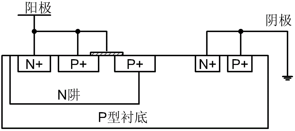
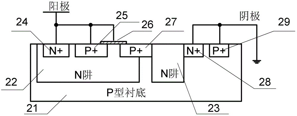
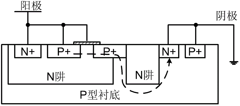
[0021] Such as figure 2 As shown, a thyristor device embedded with a P-type MOS transistor for auxiliary triggering includes a P-type substrate 21, wherein a first N-well 22, a second N-well 23, and a first N-well 23 are sequentially arranged on the P-type substrate 21. Two N+ implantation regions 28 and the third P+ implantation region 29, the first N+ implantation region 24, the first P+ implantation region 25 and the second P+ implantation region 27 are successively provided on the first N well 22, and in the first P+ implantation region 25 A polysilicon gate oxide layer 26 is bridged between the second P+ implantation region 27, and one side of the second P+ implantation region 27 extends beyond the junction of the P-type substrate 21 and the first N well 22, and is connected to the P-type substra...


PUM


Abstract

The invention discloses a controlled silicon device under auxiliary trigger of an embedded P-type MOS (Metal Oxide Semiconductor) transistor. A second N well without being connected with any potential is additionally arranged on a P-type substrate between a second P+ injection region and a second N+ injection region, thus a longitudinal base width of a parasitic NPN (Negative Positive Negative) triode can be effectively increased. By using the special characteristic of low-voltage starting of the embedded P-type MOS transistor, the controlled silicon device realizes low-voltage starting of controlled silicon, and is suitable for ESD (Electronic Static Discharge) protection requirements of most of circuits. Meanwhile, by using a manner of increasing a potential floating N well, the controlled silicon device achieves the purpose of increasing a clamp voltage of the controlled silicon. In addition, compared with the traditional method of purely depending on drawing the transverse base width of the triode, the controlled silicon device provided by the invention has higher efficiency on the area, is more beneficial to saving of a silicon wafer area and production cost, and is an economic and effective low-working-voltage-domain circuit ESD protective scheme. The controlled silicon device disclosed by the invention has the advantages of simple structure, uniform current, strong device property, stability and reliability.

Description

technical field [0001] The invention belongs to the field of integrated circuits, and in particular relates to a thyristor device used for ESD protection of integrated circuits in a low operating voltage domain. Background technique [0002] The phenomenon of electrostatic discharge (ESD) in nature poses a serious threat to the reliability of integrated circuits. In the industry, 30% of the failures of integrated circuit products are caused by electrostatic discharge, and the increasingly smaller process size and thinner gate oxide thickness greatly increase the probability of integrated circuit damage by electrostatic discharge. Therefore, improving the reliability of integrated circuit electrostatic discharge protection has a non-negligible effect on improving the yield of products. [0003] The modes of electrostatic discharge phenomena are usually divided into four types: HBM (Human Body Model), MM (Machine Discharge Model), CDM (Component Charge Discharge Model) and Fi...

Claims


Application Information

Patent Timeline
Patent Type & Authority Patents(China)
IPC IPC(8): H01L27/02H01L29/87H01L29/06
Inventor 苗萌董树荣吴健曾杰韩雁马飞郑剑锋
Owner ZHEJIANG UNIV
Why Eureka
Try Eureka