Method for manufacturing isolation cavity compatible with semiconductor process and isolation cavity

An isolation cavity and semiconductor technology, applied in the field of micro-electromechanical system manufacturing, can solve problems such as difficult thinning and inconformity with the miniaturization trend of semiconductor devices, and achieve the effects of reducing manufacturing costs, good cost advantages, and reducing wafer thickness

Active Publication Date: 2011-11-30
ADVANCED SEMICON MFG CO LTD
View PDF7 Cites 4 Cited by
  • Summary
  • Abstract
  • Description
  • Claims
  • Application Information

AI Technical Summary

Problems solved by technology

In addition, the entire thickness of the substrate where the cavity is realized by this method is very thick (the total thickness of the silicon wafer and glass), close to or exceeding 1 mm, and it is difficult to reduce the thickness, which does not conform to the miniaturization trend of semiconductor devices

Method used


Image

  • Method for manufacturing isolation cavity compatible with semiconductor process and isolation cavity
  • Method for manufacturing isolation cavity compatible with semiconductor process and isolation cavity
  • Method for manufacturing isolation cavity compatible with semiconductor process and isolation cavity

Examples


Embodiment Construction

[0046] The present invention will be further described below in conjunction with specific embodiment and accompanying drawing, set forth more details in the following description so as to fully understand the present invention, but the present invention can obviously be implemented in a variety of other ways different from this description, Those skilled in the art can make similar promotions and deductions based on actual application situations without violating the connotation of the present invention, so the content of this specific embodiment should not limit the protection scope of the present invention.

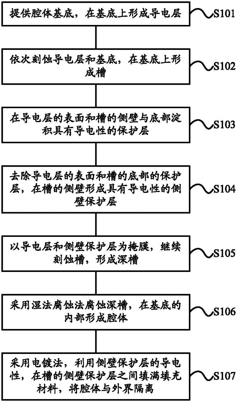
[0047] figure 1 It is a schematic flowchart of a method for manufacturing an isolation cavity compatible with a semiconductor process according to an embodiment of the present invention. As shown, the method flow may include:

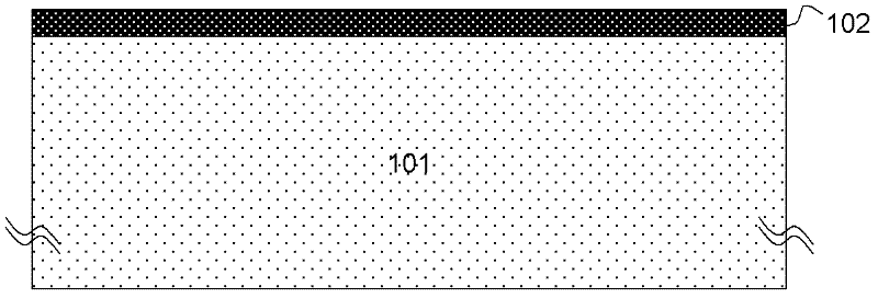
[0048] Executing step S101, providing a cavity substrate, and forming a conductive layer on the substrate;

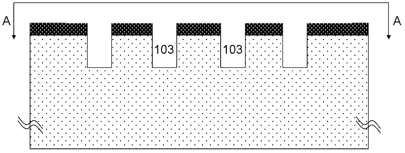
[0049] Executing step S102, seque...


PUM


Abstract

The invention provides an isolation cavity manufacturing method compatible with a semiconductor process. The method comprises the following steps of: providing a cavity substrate, and forming a conductive layer on the substrate; etching the conductive layer and the substrate in turn, and forming grooves on the substrate; depositing protection layers with conductivity on the surface of the conductive layer and the side walls and the bottoms of the grooves; removing the protection layers on the surface of the conductive layer and the bottoms of the grooves, and forming side wall protection layers with conductivity on the side walls of the grooves; continuously etching the grooves by using the conductive layer and the side wall protection layers as masks to form deep grooves; corroding the deep grooves by a wet corrosion method to form a cavity in the substrate; and filling a filling material among the side wall protection layers of the grooves by an electroplating method to isolate the cavity from outside. The invention also provides an isolation cavity. The method belongs to a front side process and is compatible with the semiconductor process; the implementation mode is simple, and wafer thickness after the cavity is formed is greatly reduced; and manufacturing cost can be reduced, the cavity has a good cost advantage, and the method is matched with the miniaturization trend of a device.

Description

technical field [0001] The invention relates to the technical field of micro-electro-mechanical system manufacturing, in particular, the invention relates to a method for manufacturing an isolation cavity compatible with a semiconductor process and the isolation cavity. Background technique [0002] In MEMS (Micro-Electro-Mechanical Systems) pressure sensors, microfluidic devices and other applications, tiny isolated cavities are important components, some of these cavities are vacuum, some are filled with specific gases or liquids. In different applications, these isolated cavities have different functions. For example, in a pressure sensor, the isolated cavities serve as the background pressure for pressure comparison. [0003] In order to realize the manufacture of cavities in the above-mentioned different applications, researchers have proposed various methods. For example, a common practice in the field of MEMS is to form grooves on one side of the silicon wafer through...

Claims


Application Information

Patent Timeline
Patent Type & Authority Applications(China)
IPC IPC(8): B81C1/00B81B1/00
Inventor 谢志峰张挺邵凯
Owner ADVANCED SEMICON MFG CO LTD
Why Eureka
Try Eureka