A homogeneous conductive paste
A technology of conductive paste and functional phase, which is applied in the field of preparation of thick film electronic paste, and can solve problems that have not been solved well
- Summary
- Abstract
- Description
- Claims
- Application Information
AI Technical Summary
Problems solved by technology
Method used
Image
Examples
Embodiment 1
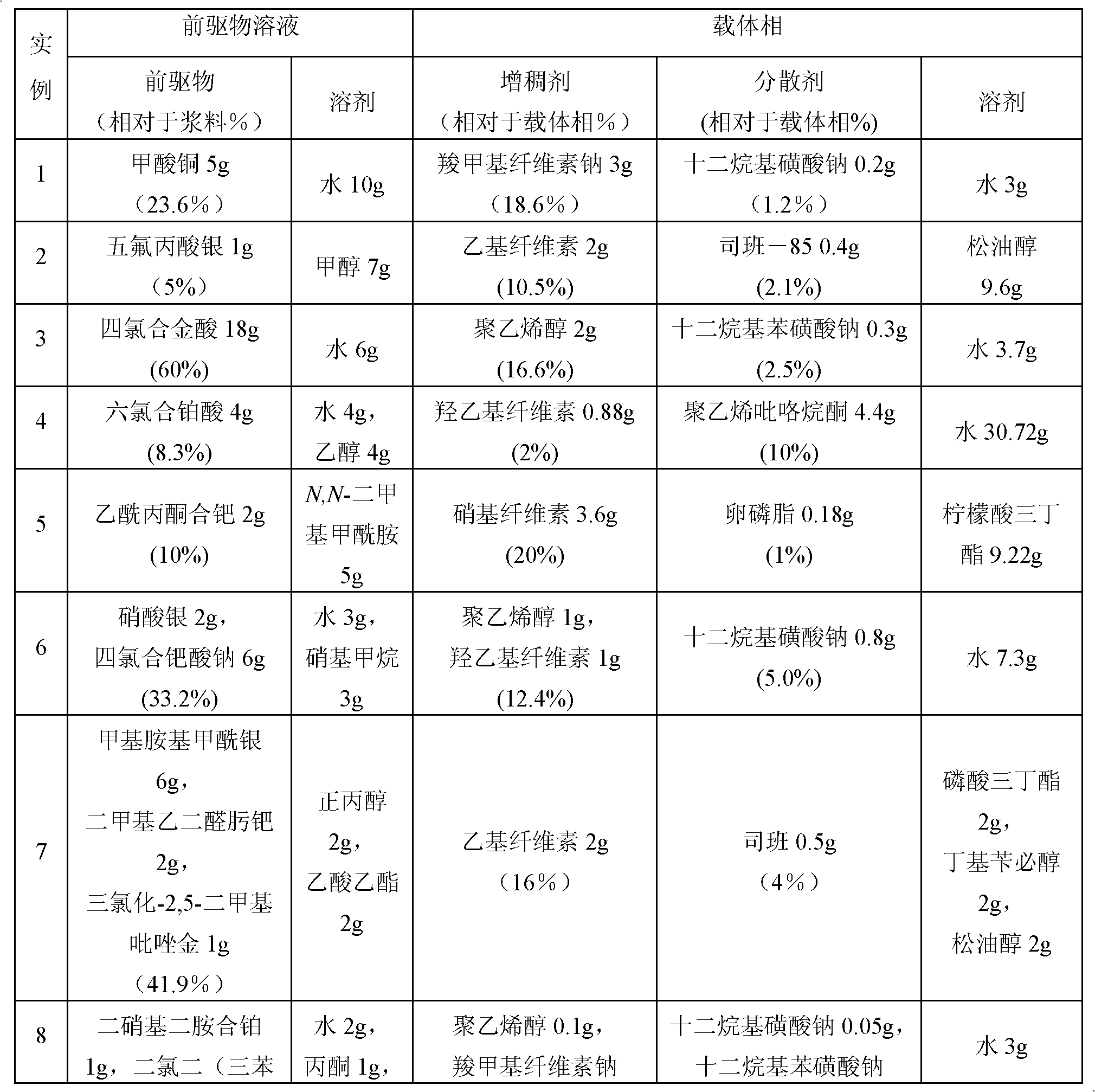
[0020] Dissolve 5 g of the precursor copper formate in 10 g of water to obtain an aqueous solution of copper formate; dissolve 3 g of sodium carboxymethyl cellulose in 3 g of water, add 0.2 g of sodium dodecylbenzene sulfonate, and dissolve to obtain a carrier phase; The aqueous solution of copper formate is mixed with the carrier, and mechanically stirred evenly to obtain the slurry of the present invention.
[0021] After the slurry was spin-coated on a quartz glass substrate to form a film, it was dried at 65°C for 30 min, and then 2 Laser or Nd:YAG treatment, can get conductive layer or conductive line, its volume resistivity is about 4.7×10 -5 Ω·cm.
Embodiment 2
[0023] Dissolve 1 g of the precursor silver pentafluoropropionate in 7 g of methanol to obtain a methanol solution of the precursor; dissolve 2 g of ethyl cellulose in 9.6 g of terpineol, add 0.4 g of Span-85 to obtain a carrier phase; Mix the methanol solution of the substance with the carrier, continue stirring evenly, and then ultrasonically disperse to obtain the slurry of the present invention.
[0024] The slurry is directly written on the ceramic substrate with a micro-pen (tip inner diameter of 20 μm) direct writing device, first dried at 50°C for 20 minutes, and then sintered at 450°C for 30 minutes to obtain a conductive pattern with a resolution of up to 20 μm Around, the volume resistivity is about 6.2×10 -5 Ω·cm.
Embodiment 3
[0026] Dissolve 18g of precursor tetrachloroalloy acid in 6g of water to obtain the aqueous solution of precursor; dissolve 2g of polyvinyl alcohol in 3.7g of water, add 0.3g of sodium dodecylbenzenesulfonate, and dissolve to obtain a carrier phase; The above-mentioned precursor aqueous solution is mixed with the carrier, and mechanically stirred evenly to obtain the slurry of the present invention.
[0027] The slurry is screen printed on the ceramic substrate, dried at 70°C for 20 minutes, and then sintered at 350°C for 40 minutes to obtain a conductive pattern with a volume resistivity of about 8.3×10 -5 Ω·cm.
PUM
| Property | Measurement | Unit |
|---|---|---|
| electrical resistivity | aaaaa | aaaaa |
| electrical resistivity | aaaaa | aaaaa |
| electrical resistivity | aaaaa | aaaaa |
Abstract
Description
Claims
Application Information


