High-current full-wafer full-crimp flat-pack IGBT and manufacturing method thereof

A manufacturing method, a flat-plate technology, applied in semiconductor/solid-state device manufacturing, circuits, transistors, etc., can solve the problem of heat dissipation, thermal shock resistance, low conduction current capability and reliability, and limit large-capacity power electronic commutation systems Application, low heat dissipation performance and thermal shock resistance, etc., achieve simple gate voltage control, improve wafer area utilization, improve thermal conductivity and thermal shock resistance

Active Publication Date: 2011-12-07
HUNAN UNIV
View PDF5 Cites 18 Cited by
  • Summary
  • Abstract
  • Description
  • Claims
  • Application Information

AI Technical Summary

Problems solved by technology

However, because the traditional IGBT module adopts the multi-chip parallel packaging method of aluminum leads and ceramic copper-clad substrates, it can only rely on low-layer ceramic substrates for heat dissipation, and its heat dissipation performance, thermal shock resistance, conduction current capability and reliability are all poor. Thyristors or IGCTs below equivalent voltage classes
These shortcomings of IGBT limit its application in large-capacity power electronic converter systems
In recent years, a small number of IGBT manufacturers have also tried to use double-sided heat dissipation pressure contact (press-fit) IGBT packaging, but due to the structural constraints of IGBT multi-chip parallel connection, its cost is greatly exceeded, while the heat dissipation performance and thermal shock resistance are poor. Lower than traditional thyristor double-sided pressure contact planar package

Method used


Image

  • High-current full-wafer full-crimp flat-pack IGBT and manufacturing method thereof
  • High-current full-wafer full-crimp flat-pack IGBT and manufacturing method thereof
  • High-current full-wafer full-crimp flat-pack IGBT and manufacturing method thereof

Examples


Embodiment Construction

[0030] The present invention will be further described below in conjunction with the accompanying drawings and specific embodiments.

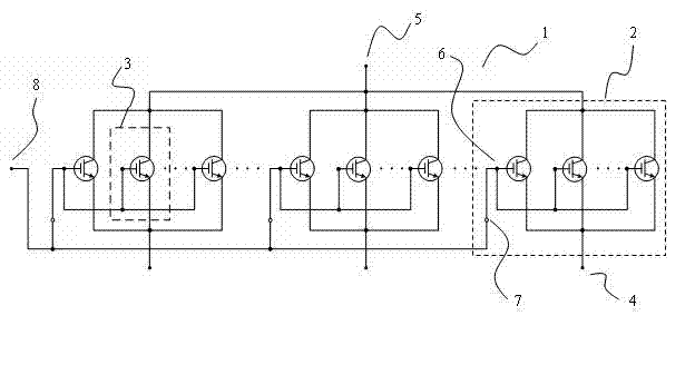
[0031] Each known conventional IGBT wafer contains dozens to hundreds of identical IGBT chips, and these IGBT chips will be cut into rectangular independent chips after the semiconductor wafer process and testing are completed. Each IGBT chip is usually composed of thousands of IGBT units connected in parallel, and the emitter, gate and collector of each unit are connected together through metal or polysilicon film. In addition, part of the chip area of ​​each IGBT chip along its edge is used as an edge electric field stop area to ensure the breakdown voltage of the device.

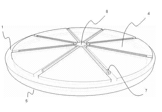
[0032] The present invention provides a large current whole wafer IGBT device, the circuit of which is as follows: figure 1 shown. As a single device, the IGBT wafer 1 is composed of a plurality of independent IGBT device regions 2 , and each IGBT device region 2 is com...


PUM


Abstract

The invention discloses a heavy-current whole-wafer total-pressure-contact flat-plate encapsulated IGBT (Insulated Gate Bipolar Transistor) and a manufacturing method thereof. The heavy-current whole-wafer total-pressure-contact flat-plate encapsulated IGBT comprises an IGBT whole wafer and a total-pressure-contact flat-plate encapsulation, the whole wafer comprises multiple independent IGBT device regions, each IGBT device region is composed of multiple IGBT units which are connected in parallel, collectors of all the IGBT device regions are connected in parallel to form a total collector, atransmitter is led from each IGBT device region independently, gate poles of all the IGBT device regions in a normal operating state are connected to a total gate pole arranged in the center of the wafer by using an interconnecting line, and the transmitter of each IGBT device region is connected with a metal electrode plate of a total transmitter in parallel by virtue of a metal gasket of the transmitter. According to the invention, a heavy-current IGBT whole wafer device is realized, the advantages of high working voltage, low switching power consumption and simple voltage control of the gate pole are maintained, current carrying capacity, heat-conducting property, heat shock resistance and long-term reliability of the device are improved, and the problem of property matching between IGBT units is solved.

Description

technical field [0001] The invention relates to an IGBT device, in particular to an IGBT packaged in a high-current full-wafer full-press-bonded flat-panel package and a manufacturing method thereof. Background technique [0002] High-power power semiconductor switching devices including thyristors and insulated gate bipolar transistors (IGBTs) are widely used in motor energy saving, new energy, power transmission and transformation, rail transit, metallurgy, chemical industry and other fields. One of the key technologies indispensable to a friendly society. The performance requirements for such devices generally include: high voltage (3300 to 10000 volts), high current (500 to 5000 amperes), low conduction and switching power consumption, good switch controllability, large safe working area, Good thermal conductivity, thermal shock resistance and long-term reliability. However, the existing high-power power semiconductor switching devices have the following deficiencies:...

Claims


Application Information

Patent Timeline
Patent Type & Authority Applications(China)
IPC IPC(8): H01L27/102H01L21/8222
Inventor 沈征帅智康罗安尹新
Owner HUNAN UNIV
Why Eureka
Try Eureka