Method for preparing high-resistance transparent zinc oxide (ZnO) thin film by utilizing direct current magnetic control sputtering equipment

A high-resistance, thin-film technology, used in sputtering, metal material coating, vacuum evaporation, etc., can solve problems such as difficulty in large-scale production, affecting the performance of solar cells, and complex processes

Active Publication Date: 2012-01-11
山东中科泰阳光电科技有限公司
View PDF5 Cites 10 Cited by
  • Summary
  • Abstract
  • Description
  • Claims
  • Application Information

AI Technical Summary

Problems solved by technology

However, too high oxygen content in the plasma can cause damage to the inner pre-film [(12) T.Nakada, M.Mizutani, Jpn.J.Appl.Phys.41(2002) L165; (13) K. Kushiya, T.Nii, etc.Jpn.J.Ap

Method used


Image

  • Method for preparing high-resistance transparent zinc oxide (ZnO) thin film by utilizing direct current magnetic control sputtering equipment
  • Method for preparing high-resistance transparent zinc oxide (ZnO) thin film by utilizing direct current magnetic control sputtering equipment
  • Method for preparing high-resistance transparent zinc oxide (ZnO) thin film by utilizing direct current magnetic control sputtering equipment

Examples


Embodiment 1

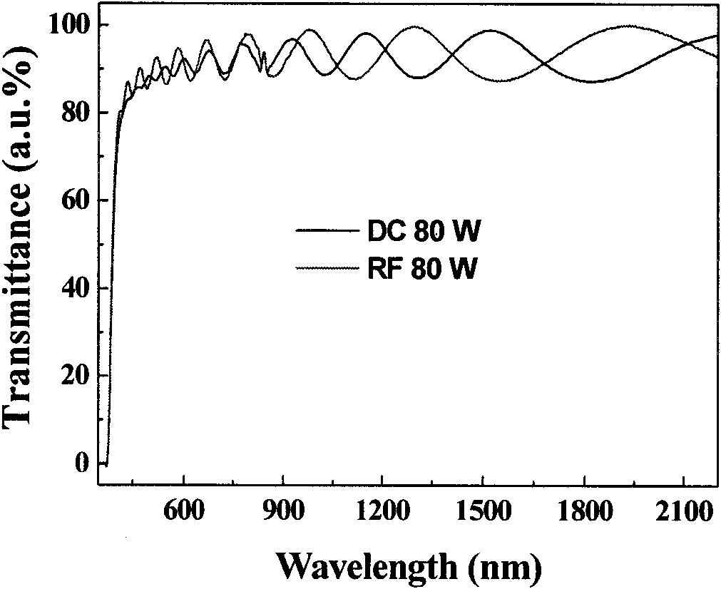
[0026] Adopt rich Zn (or lack O 2 ) ZnO target material (application in another case), using DC magnetron sputtering, ordinary glass as the substrate, and the background vacuum is pumped to 2.0×10 -4 Pa, with high purity argon as the working gas, and a small amount of O 2 (O 2 The volume percentage of the total gas flow is 0.5%), the working pressure is maintained at 1.2Pa, the distance between the target and the substrate is set to 7cm, the sputtering power is 80W, and the deposition time is 40min. In addition, for the sake of comparison, a commercial intrinsic ZnO ceramic target was used, and the radio frequency magnetron sputtering method was used to sputter for 60 minutes under the same background vacuum, atmosphere, pressure, and target distance. The thickness of the film samples prepared under the two conditions are both 800 nm.

[0027] figure 1 The transmission spectra of the ZnO film samples prepared under the two conditions. It can be seen that the average transmittance...

Embodiment 2

[0030] In the application of thin-film solar cells and optoelectronic devices, the thickness of the high-resistance ZnO film is generally controlled between 60 and 120 nm. In this example, sintering at a sintering temperature of 850°C for 20 hours was used to obtain zinc-rich Zn 1.13 O-structure wide-gap ceramic material target material, using DC magnetron sputtering, ordinary glass as the substrate, the background vacuum is pumped to 2.0×10 -4 Pa, with high purity argon as the working gas, and a small amount of O 2 (O 2 0.5% of the total gas flow), the working pressure is maintained at 1.2Pa, the distance between the target and the substrate is set to 7cm, the sputtering power is 80W, and the deposition time is 4min. The thickness of the prepared film sample is 80nm.

[0031] Figure 5 For the transmission spectrum of the prepared ZnO film sample, it can be seen that the average transmittance of the film in the visible light region reaches nearly 90%, and even in the near-infrare...

Embodiment 3

[0033] Adopt rich Zn (or lack O 2 ) ZnO target material, using DC magnetron sputtering, ordinary glass as the substrate, the background vacuum is pumped to 2.0×10 -4 Pa, using pure high-purity argon as the working gas, the working pressure is maintained at 1.2 Pa, the distance between the target and the substrate is set to 7 cm, the sputtering power is 80 W, and the deposition time is 4 min. The thickness of the prepared film sample is 80nm. The electrical performance test results show that the resistivity of the sample prepared under the conditions of this embodiment is about 7×10 5 Ω·cm, slightly lower than Example 2, the average transmittance from visible light to near-infrared region (400-2200nm) is about 90%, which is equivalent to Example 2, which is in line with the thin film solar cell window layer, diffusion barrier layer and others Application requirements for optoelectronic devices.


PUM

PropertyMeasurementUnit
Resistivityaaaaaaaaaa

Abstract

The invention relates to a method for preparing a high-resistance transparent zinc oxide (ZnO) thin film by utilizing direct current magnetic control sputtering equipment, which is characterized in that based on Zn-rich (or O2-inefficient) zinc oxide-based wide bandgap ceramic material target, direct current magnetic control sputtering is utilized to replace traditional radio frequency magnetic control sputtering to prepare the high-resistance ZnO-based transparent thin film, and the transparent thin film is used for the diffusion barrier layers and the window layers of thin film solar cells. Through regulating technological parameters, the resistivity of the prepared high-resistance ZnO-based transparent thin film can be controlled to be within the range of 104-108omega.cm, and the average transmissivity in visual and near infrared zones is about 90 percent. Compared with the high-resistance ZnO-based thin film prepared a radio frequency magnetic control sputtering method based on a commercial intrinsic ZnO ceramic target, under the condition of same film thickness, the transmissivity, the resistivity and the surface toughness are equivalent to those of the thin film prepared by the method of the invention. The high-resistance transparent zinc oxide (ZnO) thin film has a simple preparation process, low cost and high transparency in the visual and near infrared zones, and can be widely applied to the field of transparent electronics and novel photoelectric devices, especially the thin film solar cells.

Description

Technical field [0001] The invention relates to a method for preparing a high-resistance transparent ZnO-based film by using direct current magnetron sputtering. It belongs to the technical field of transparent conductive film materials (TCM). Background technique [0002] High-resistance transparent ZnO film has broad application prospects in the field of transparent electronics and new optoelectronic devices. In thin-film solar cells and optoelectronic devices, ZnO films with controllable resistance within a certain range and high transmittance can be used as window layers and diffusion The barrier layer can significantly improve the uniformity and stability of the thin film battery. In amorphous silicon, microcrystalline silicon and CdTe thin-film solar cells, a thin layer of high-resistance transparent ZnO film is deposited between the back electrode and the N-type light absorption layer, which can be used as a diffusion barrier [(1) AVShah, H. Schade, et al. Progress in Ph...

Claims


Application Information

Patent Timeline
IPC IPC(8): C23C14/08C23C14/35
Inventor 黄富强万冬云汪宙
Owner 山东中科泰阳光电科技有限公司
Why Eureka
Try Eureka