Method for measuring electric parameter of gallium arsenide pseudomorphic HEMT (high electron mobility transistor) material

A technology of high electron mobility and measurement method, which is applied in the field of electrical parameter measurement of gallium arsenide pseudo-matching high electron mobility transistor materials, and can solve the problem that the electrical properties of materials cannot be truly and completely reflected.

Inactive Publication Date: 2012-01-11
HEBEI UNIV OF TECH
View PDF4 Cites 4 Cited by
  • Summary
  • Abstract
  • Description
  • Claims
  • Application Information

AI Technical Summary

Problems solved by technology

[0006] The technical problem to be solved by the present invention is to provide a method for measuring the electrical parameters of gallium arsenide-based high electron mobility transistor materials, which is a non-destructive, convenient, efficient and accurate measurement of gallium arsenide-based biplane doping pseudo-high The method of carrier concentration and mobility in the electron mobility transistor material overcomes the cumbersome and inefficient preparation process of the sample to be measured in the existing measurement method, and at the same time, the introduction of the electrode and the destruction of the sample will also bring some Errors, and the electrical parameters measured by the fixed magnetic field method are only the result of a comprehensive effect, and cannot truly and completely reflect the shortcomings of the electrical properties of the material

Method used


Image

  • Method for measuring electric parameter of gallium arsenide pseudomorphic HEMT (high electron mobility transistor) material
  • Method for measuring electric parameter of gallium arsenide pseudomorphic HEMT (high electron mobility transistor) material
  • Method for measuring electric parameter of gallium arsenide pseudomorphic HEMT (high electron mobility transistor) material

Examples


Embodiment 1

[0043] Preparation of GaAs-based double delta-doped PHEMT materials.

[0044] The preparation technology is prepared by molecular beam epitaxy. The steps are: after the GaAs(100) substrate is loaded into the system, it is pre-degassed at 90°C and 150°C in the fast sampling chamber, and then introduced into the pretreatment chamber. After the degassing is completed at ℃, it is introduced into the growth chamber. At 630℃, As 2 Under the protection of atmosphere, deoxidize the surface for 10 minutes, and grow when the temperature drops to 580°C The GaAs buffer layer, and then continue to grow other layers of materials, the As / Ga beam current ratio is 17-20, and the growth rate is 1μm / hour; during the growth of the InGaAs channel layer, the substrate temperature is controlled at about 480°C to reduce In segregation phenomenon. The temperature of the In source furnace is 760°C, and the growth time of the channel layer is about 30 seconds; the Al composition is controlled to be 0...

Embodiment 2

[0048] Preparation of Test Samples of GaAs Pseudomorphic High Electron Mobility Transistor Material

[0049] Using the process of Example 1, three groups of gallium arsenide pseudomorphic high electron mobility transistor material test samples were prepared, with two pieces in each group.

[0050] Group A: 2# tested samples, including two pieces of E and F. The 2# tested sample was prepared by the flat heterojunction interface growth technology in the process of Example 1, that is, the growth process of the InGaAs channel layer was optimized by temperature control and interfacial growth pause method in the preparation to obtain a flat interface. The 2# tested sample has a thin cap layer structure.

[0051] Group B: 3# tested samples, including two pieces of G and H. The 3# tested sample was prepared in the process of Example 1 using common process technology, that is, the common process was used in the growth process of the InGaAs channel layer. The 3# tested sample is a fu...

Embodiment 3

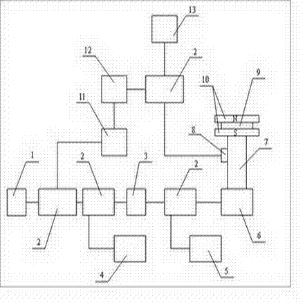
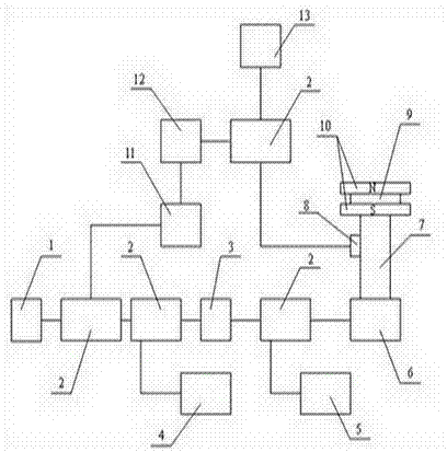
[0057] Adopt the microwave Hall measuring device shown in the accompanying drawing, use the method of the present invention to measure the carrier concentration of the 2-dimensional electron gas (2DEG) in the sample channel layer of the above-mentioned each group of measured gallium arsenide pseudo-alternative high electron mobility transistor materials and Hall mobility.

[0058] 3-1.Measurement of electrical parameters of 2#E piece of test sample in group A

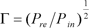
[0059] The first step is to use a microwave Hall measuring device to measure the incident power, reflected power and Hall effect microwave power of the gallium arsenide pseudofabricated high electron mobility transistor material to be measured

[0060] The 2#E sheet measured sample made by embodiment 2 is placed on the sample stage 9 in the microwave Hall measuring device, and the 10GHz and TE emitted by the 10GHz microwave source 1 are transmitted by the circular waveguide 7 of the balance modulation. 11 The microwave...


PUM


Abstract

The invention discloses a method for measuring an electric parameter of a gallium arsenide pseudomorphic HEMT (high electron mobility transistor) material and relates to a method for measuring the electric parameter of a semiconductor material. The method is used for measuring a carrier concentration and a mobility in the gallium arsenide pseudomorphic HEMT material by a non-contact Hall measurement method and comprises the following steps of: measuring an incident power, a reflection power and a Hall effect microwave power of the measured gallium arsenide pseudomorphic HEMT material by a microwave Hall measurement device; calculating conductance tensors of a measured sample in different magnetic fields; and calculating the carrier concentration and the mobility of the gallium arsenide pseudomorphic HEMT material. The method disclosed by the invention is nondestructive, is convenient and rapid, has high efficiency and can be used for accurately measuring the carrier concentration and the mobility in the gallium arsenide-based biplane doped pseudomorphic HEMT material. The defects that the existing measurement method is fussy to operate, has low efficiency and a certain error and cannot really and completely reflect the electrical properties of the material are overcome.

Description

technical field [0001] The technical solution of the invention relates to a method for measuring electrical parameters of semiconductor materials, in particular to a method for measuring electrical parameters of gallium arsenide pseudomorphic high electron mobility transistor materials. Background technique [0002] Gallium arsenide (hereinafter referred to as GaAs) based biplane (hereinafter referred to as double δ) doped AlGaAs / InGaAs pseudo-high electron mobility transistor (hereinafter referred to as PHEMT) due to its high power, high efficiency, excellent linearity and can be used in relatively It is widely used in technical fields such as phased array radar, satellite communication, wireless local loop and personal communication system due to its characteristics of normal operation in a large voltage range; PHEMTT devices have good power and efficiency characteristics especially at the high end of millimeter wave, making It has become a mainstream device for millimeter...

Claims


Application Information

Patent Timeline
Patent Type & Authority Applications(China)
IPC IPC(8): G01R19/08G01R29/12G01R27/02
Inventor 杨瑞霞王伟武一宾牛晨亮
Owner HEBEI UNIV OF TECH
Why Eureka
Try Eureka