Solid state relay
A solid state relay and relay technology, applied in electrical components, electronic switches, pulse technology, etc., can solve problems such as poor anti-interference ability, insufficient control, increased chip area and wiring difficulty, etc., to achieve strong anti-interference ability, increase area, The effect of speeding up the bleeder circuit is simple
- Summary
- Abstract
- Description
- Claims
- Application Information
AI Technical Summary
Problems solved by technology
Method used
Image
Examples
Embodiment 1
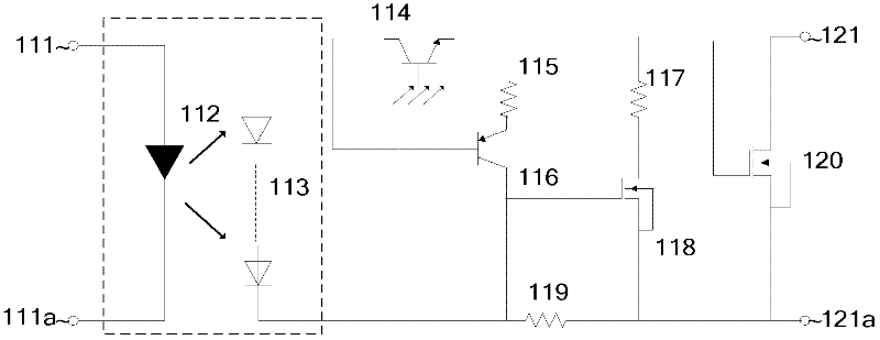
[0029] An embodiment of the solid state relay according to the present invention is as figure 1 Shown in Example 1. Including, a light-emitting element 112 connected between the relay input terminals 111 and 111a; a photovoltaic diode array 113 that generates photovoltaic output when coupling the light signal of the light-emitting element; a normally open metal oxide field connected between the relay output terminals The effect transistor 120 also includes,
[0030] A charging circuit composed of a phototransistor 114 and a resistor 119, wherein the emitter of the phototransistor 114 is connected to the gate of the output normally-on metal oxide field effect transistor 120, the collector is connected to the first end of the photovoltaic diode array 113, and the resistor 119 is connected between the source of the output normally-on metal oxide field effect transistor 120 and the second end of the photovoltaic diode array 113; here, the base of the phototransistor 114 is suspen...
Embodiment 2
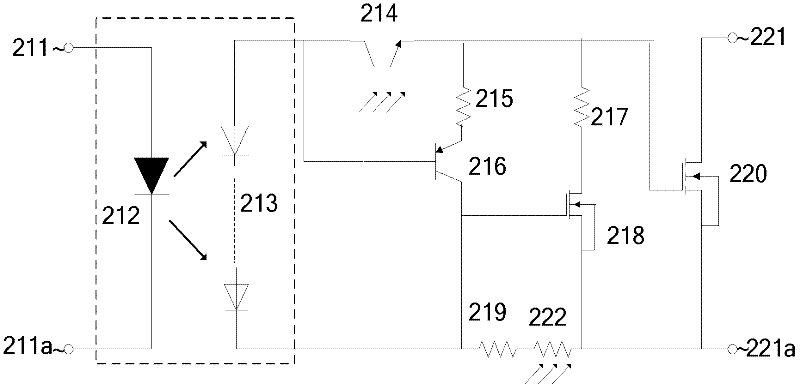
[0044] refer to figure 2 shows another circuit configuration, this circuit is in figure 1 On the basis of the shown circuit, a photoresistor 222 is supplemented on the branch where the resistor 219 is located. According to the previous analysis, figure 1 The function of the resistor 119 in the shown circuit is to ensure that the N-channel depletion-type MOSFET 118 is in a cut-off state when the gate of the output MOSFET 120 is charged (this determines the minimum value of the resistor 119) , while in the initial stage of discharging the gate charge of the output mosfet 120 (ie t d stage) the presence of the resistor 119 improves the gate-source bias of the N-channel depletion-mode MOSFET 118, thereby increasing the drain-source current. figure 2 The photoresistor 222 added in the middle circuit is in a low-resistance state when receiving light, and is in a high-resistance state when there is no light, so that when charging the gate of the output metal oxide field effect t...
Embodiment 3
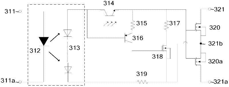
[0046] image 3 It is a circuit application scheme when there are two output metal oxide field effect transistors. The sources of the two normally-on metal oxide field effect transistors 320 and 320a are connected to serve as the third output terminal of the relay; the two drains serve as the first and second output terminals of the relay respectively. This circuit structure can be used in an AC environment, and only one of the metal oxide field effect transistors works in each half current cycle. The working principles of the charging circuit and the accelerated discharge circuit are the same as those of the first embodiment above, and will not be described again.
PUM
 Abstract
Description
Claims
Application Information


