Quad flat non-lead (QFN) package with high density and manufacturing method

A leadless encapsulation, flat four-sided technology, used in semiconductor/solid-state device manufacturing, electrical components, electrical solid-state devices, etc., can solve the problems of limited solder coverage, inability to meet high density, delamination failure, etc. Combine quality and surface mount quality, prevent metal burrs, and increase fatigue life

Inactive Publication Date: 2012-02-15
BEIJING UNIV OF TECH
View PDF8 Cites 22 Cited by
  • Summary
  • Abstract
  • Description
  • Claims
  • Application Information

AI Technical Summary

Problems solved by technology

[0004] With the improvement of IC integration and the continuous enhancement of functions, the number of I/Os of ICs increases, and the number of I/O pins of corresponding electronic packages also increases accordingly. The pins of the ring are arranged around the chip carrier, which limits the increase in the number of I/Os and cannot meet the needs of high-density ICs with more I/Os.
The traditional lead frame has no step structure design, which cannot effectively lock the plastic material, resulting in low bonding strength between the lead frame and the plastic packaging material, which is easy to cause delamination of the lead frame and the plastic packaging material or even the falling off of the pin or chip carrier, and cannot effectively Prevent moisture from diffusing into the electronic package along the interface between the lead frame and the plastic packaging material, which seriously affects the reliability of the package
The chip carrier and outer pins of traditional QFN products do not have a certain raised part,

Method used


Image

  • Quad flat non-lead (QFN) package with high density and manufacturing method
  • Quad flat non-lead (QFN) package with high density and manufacturing method
  • Quad flat non-lead (QFN) package with high density and manufacturing method

Examples


Embodiment Construction

[0067] The present invention is described in detail below in conjunction with accompanying drawing:

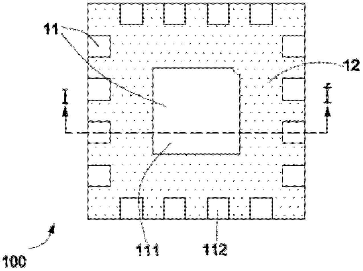
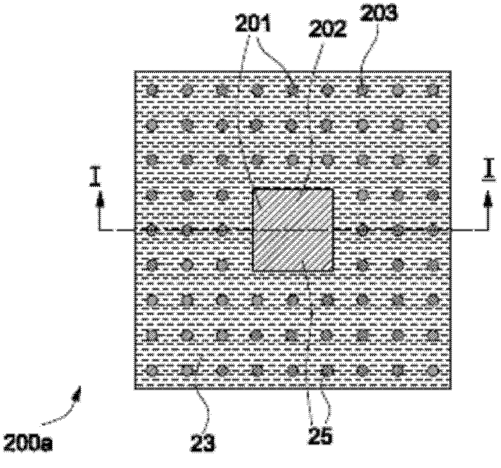
[0068] Figure 2A A schematic diagram of the rear side of a high-density QFN package structure in which the cross-section of the pins is circular and the pins on each side of the chip carrier are arranged in parallel according to an embodiment of the present invention. Figure 2B A schematic diagram of the rear side of a high-density QFN package structure in which the cross-section of the pins is rectangular and the pins on each side of the chip carrier are arranged in parallel according to the embodiment of the present invention.

[0069] Refer to the above Figure 2A -B It can be seen that, in this embodiment, the lead frames 201 of the high-density QFN package structures 200a and 200b include a chip carrier 202 and pins 203 arranged in multiple circles around the chip carrier 202, and the leads 203 on each side of the chip carrier 202 The pins 203 are arranged in parallel...


PUM


Abstract

The invention discloses a quad flat non-lead (QFN) package with high density and a manufacturing method. The package comprises a lead frame 201, metal material layers 25, an IC chip 27, insulating filling materials 23, bonding materials 26, metal conductors 28 and plastic package materials 29, wherein the lead frame comprises a chip carrier 202 and a plurality of leads 203 arranged in multiple circles around the chip carrier; the metal material layers are arranged on the upper and lower surfaces of the lead frame; the IC chip is arranged on a metal material layer on the upper surface of the lead frame; the insulating filling materials are arranged below stepped structures 22b of the lead frame; the bonding materials are arranged between the IC chip and the metal material layer on the upper surface of the lead frame; the IC chip is connected to the inner leads of the multiple circles of leads and the upper surface of the chip carrier respectively by the metal conductors; the plastic package materials wrap and seal the IC chip, the bonding materials, the metal conductors, partial regions of the lead frame and partial metal material layers; and the chip carrier and the outer leads exposed out of the bottom surface of a package structure, are provided with raised parts. The package and the manufacturing method have the following beneficial effects: the bottleneck of low I/O quantity is broken through and the package reliability is improved.

Description

technical field [0001] The invention relates to the technical field of manufacturing semiconductor components, in particular to a high-density four-sided flat no-lead package, and the invention also includes a manufacturing method of the package. Background technique [0002] With the development of electronic products such as mobile phones and notebook computers towards miniaturization, portability, ultra-thinness, multimedia and low-cost requirements for popularization, high-density, high-performance, high-reliability and low-cost packaging forms and Its assembly technology has been developed rapidly. Compared with the expensive BGA and other packaging forms, the new packaging technology developed rapidly in recent years, that is, the quad flat non-lead QFN (Quad Flat Non-lead Package) package, due to its good thermal performance and electrical performance, small size, Many advantages such as low cost and high productivity have triggered a new revolution in the field of m...

Claims


Application Information

Patent Timeline
IPC IPC(8): H01L23/495H01L23/31H01L21/48H01L21/56
CPCH01L24/97H01L24/73H01L2224/32245H01L2224/48247H01L2224/73265H01L2224/92247H01L2224/97H01L2924/14H01L2924/181H01L2924/30107H01L2924/3011H01L2224/85H01L2924/00012H01L2924/00
Inventor 秦飞夏国峰安彤武伟刘程艳朱文辉
Owner BEIJING UNIV OF TECH
Why Eureka
Try Eureka